
Going for GaN
GaN HEMTs are the latest in RF and microwave power transistor technology. They are quickly gaining favor for many applications because of their high gain and high-power levels at S-Band and above. GaN power transistors are most often produced on a SiC substrate which offers excellent heat extraction for enhanced long term reliability although a couple of companies are offering GaN on Si.
GaN HEMTs are ideally suited to high-power pulsed applications and their power density requirements (as compared to CW applications) as the ability to design on a SiC substrate allows for optimal cooling. Because of this superior power, the output capacitance per Watt will be much lower. This enables designers to implement harmonic tuning with output with efficiencies > 85 percent—even at kW power levels. The much lower capacitance per Watt is also what enables these devices to operate at much higher frequencies than possible with LDMOS. One disadvantage of GaN HEMTs, however, is that they are typically depletion-mode devices, which means not only that they require both positive and negative voltage supplies, but the gate voltage must also be applied before the drain voltage. To address this pitfall, some companies implement GPS circuitry in their pallets and test fixtures, which minimizes this issue and its impact on the BOM.
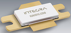
Figure 3 GaN on SiC power transistor capable of 1250 W pulsed output power under Mode S ELM for IFF/SSR applications at 1030 or 1090 MHz.
Figure 3 is an example of a state-of-the-art GaN HEMT device. This transistor typically delivers > 1250 W output power at both 1030 and 1090 MHz for IFF/SSR applications using the same circuit (a consequence of the low capacitance per Watt) along with 17 dB gain and a high 85 percent efficiency under Mode S ELM waveform (48 × {32 μs on, 18 μs off}, 6.4 percent long-term duty cycle).
Picking the Right Transistor Technology
The requirements of an application, such as waveform type, frequency, bandwidth and output-power level, will determine the type of performance needed by a power amplifier and its power transistors. At lower frequencies, all the transistor technologies discussed are viable candidates and the choice of which to use will depend upon what is most important in the design. At S-Band and above, GaN HEMTs on SiC are really the optimal choice. In between, the challenge is to balance cost versus performance which becomes trickier and experts advise starting with those solutions already defined by the industry as being ideally suited for either pulsed or CW designs and optimize from there. Table 1 summarizes the advantages and disadvantages of the three transistor technologies considered.
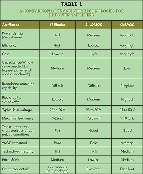
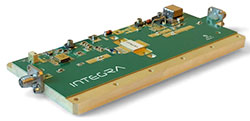
Figure 4 Low-profile RF Power Modules or “pallets” include RF matching, power-supply circuitry and control circuitry to ease the integration of a power transistor into a power amplifier design.
Another consideration is that devices are available with and without internal impedance matching and in different package styles. In addition, many of these power transistors covered here are also available as integrated PCB assemblies, RF Power Modules or “pallets.” These integrated low-profile boards include RF matching, power-supply circuitry and control circuitry (see Figure 4) to ease the integration into the RF power amplification system even further. This can simplify the system designer’s burden since they are drop-in blocks.
Conclusion
How the specifications for the choice of RF power transistors are prioritized will depend on the performance and budget requirements of a designer’s HPA. The most expensive transistors could very well be worth the investment in what they return to the total system costs. Frequency range and bandwidth, and whether the amplifier will be handling pulsed or CW signals are your first decisions, but those requirements will only help narrow down the best power transistor technology and the device for the job so much. Understanding the impacts throughout the HPA’s block diagram are essential and identifying bonus features and smart design choices your transistor supplier has made can become make or break differences.
It all really comes down to deciding early on how far the radar signal must travel, at what frequency and with what level of resolution. This will determine how far a designer is willing to stretch the budget of power transistor devices in the block diagram. Get the price/performance tradeoffs right and the system will have the power needs to accomplish its goals.