
Stabilization of RF Parameters of Injection-locked Pulsed IMPATT Oscillators
The methods for RF parameter stabilization of injection-locked pulsed impact avalanche and transit time (IMPATT) oscillators during a pulse width over the locking band in a wide range of ambient temperatures are described. A combination of current compensation and preheating of the semiconductor diode junction provides stability of the output signal amplitude and phase. The scheme for pulse preheating with high pulse rate and low additional consumed power is considered.
L.V. Kasatkin and N.F. Karushkin
Science Research Institute Orion
Kiev, Ukraine
The essential features of power pulsed IMPATT oscillators that require improvement include variation of diode junction temperature within the pulse width; and operation with high density of pulse bias current and, as a consequence, the approach of the avalanche resonant diode frequency to the oscillator's operating frequency. These pointed features lead to considerable change in diode RF impedance during the pulse width over the ambient temperature range and, as a result, to variation of the output signal amplitude and phase.
Most instabilities take place at lower junction temperatures, particularly at the leading edge of the bias current pulse. Phase instabilities Df (t) (phase chirp) rule out the strict realization of a synchronous mode of the pulse injection-locked oscillator because the frequency of the output signal fout = f0 + Df (t)/dt during the pulse width is not equal to the frequency f0 of the input signal. The output signal is coherent if the input locking signal frequency has high stability. The well-known method of RF parameter stabilization (called the current compensation method of IMPATT admittance vs. temperature changes1 ) decreases the pulsed IMPATT oscillator instabilities. However, this method, as shown in this article, does not provide full compensation (especially at low semiconductor temperatures) and only minimizes admittance changes. In this connection the requirements of high stability of RF parameters cannot be fulfilled for many applications. In addition, for RF parameter stabilization over a wide range of ambient temperatures  am , the pulse bias current amplitude must be changed, essentially leading to large variations of power output and decreasing the power level at low temperatures. An alternative method of RF parameter stabilization over an ambient temperature range is based on additional preheating of the semiconductor junction, which maintains the diode temperature practically constant, independent from ambient temperature variations.2 In this case RF parameter stabilization during the pulse width is achieved by using the current compensation method. Joint use of these two stabilization methods, namely, current compensation and additional preheating, provides much improved stability of the pulsed IMPATT oscillator's RF parameters. This article discusses the problem of attaining RF parameter stability of a pulsed injection-locked IMPATT oscillator and considers the scheme for preheating realization with high pulse rate and low power consumption.
CURRENT COMPENSATION OF IMPATT DIODE ADMITTANCE TEMPERATURE CHANGES
It is known that RF parameter instability of an IMPATT oscillator output signal during the bias current pulse width depends on the measure of current compensation of diode admittance change with temperature. However, the condition of compensation D Yd /Yd = 0 is not fulfilled exactly over a wide range of temperatures, pulse bias current amplitudes and signal amplitudes. Achieving a minimum D Yd /Yd , as a result of current compensation, is defined in this article on the basis of numerical calculations of the complex admittance of Si IMPATT diodes with a p+ p n n+ structure and optimum doping profile at an 8 mm wavelength where the lengths of p and n layers lp = 0.8 µm, ln = 1.0 µm and the doping concentration in the p and n layers is Na = 3.5 * 1016 cm3 and Nd = 3.0 * 1016 cm3 , respectively.
Figure 1 shows the calculated results of changes in diode admittance D Y1 = Y1 (390 K, I01 ) Y1 (500 K, 16 kA/cm2 ) for a diode temperature change of 500 to 390 K where Y1 is the admittance of a diode structure with p-n junction area Spn = 1 cm2 . For a diode temperature = 500 K the bias current density is J0 = 16 kA/cm2 and current compensation in the described temperature interval is achieved by increasing the current density in the limits of 12 ¾ J0 ¾ 16 kA/cm2 ; curves 1,2,3 in the data plot correspond to fixed voltage amplitudes at the diode terminals of Um = 10, 15, 20 V, respectively. It may be seen that minimum values |D Y1 |min at = 390 K are achieved for J0 = 12.5 to 13.5 kA/cm2 and diode voltage amplitudes Um = 10 to 20 V; the minimum noncompensated value |D Y1 |min = 25 to 55 S/cm2 . In comparison with a noncompensated D Y1 at = 390 K and J0 =16 kA/cm2 , the current compensation decreases the amount of diode admittance change with temperature by six to seven times. When the diode temperature increases, the results of current compensation improve. Therefore, when the diode temperature changes from = 500 K to = 590 K and the bias current density increases simultaneously to 18 to 19 kA/cm2 (instead of the initial value J0 = 16 kA/cm2 ), the noncompensated values |D Y1 | < 5 S/cm2 in the diode voltage range of Um = 10 to 20 V. This result is due to the fact that the diode avalanche resonant frequency approaches the operating frequency when the temperature is decreased. Incomplete compensation of a diode admittance change at a fixed ambient temperature is the cause of the output signal amplitude and phase variations within the pulse width.

STABILIZATION OF IMPATT DIODE JUNCTION TEMPERATURE
The design of a diode preheating system that provides a constant diode temperature *0 at the leading edge of the bias current pulse requires the use of a diode temperature sensor and automatic preheating control of the current parameters. To accomplish this control, the temperature of the diode heat sink is measured.2 This solution is not expedient for stabilization of initial diode temperature 0 when factors affecting the diode temperature change at a high pulse rate (as in the case of pulse-code modulation of diode bias current).
The solution that is used in this article is based on measuring the avalanche breakdown voltage Ubr and controlling the preheating current parameters in such a manner that at the leading edge of each bias current pulse Ubr = Ubr ( 0 ) = Ubr o = constant over all the factors that affect diode temperature. The avalanche breakdown voltage stability is equivalent to the stability of the initial temperature 0 . The operating principles of the preheating system considered here are shown in Figure 2 . The time dependencies of a diode pulse bias current I0 (t), diode voltage Ud (t) and pulse preheating current Ipr (t) are defined for constant parameters of pulse bias current; that is, pulse width  1 and pulse period T. The diode bias current I0 (t) = I0 + I0 (t) varies with regard to pulse width in accordance with principles of current compensation. The diode voltage Ud (t) varies during the pulse width from Ud0 = Ubr 0 to Ud max . After the current pulse ends at time tp = 1 + f1 + f2 , the diode voltage is Ud (tp ) = Ubr0 [1 + ß
 max ] where D max is due to diode heating during the bias current pulse. After the time interval t1 the diode temperature is *1 and the avalanche breakdown voltage related to this temperature is Ubr (t1 , 1 ), which is smaller than Ubr 0 . At tpr = tp + t1 the pulse preheating current Ipr switches on and its amplitude is proportional to D U = D Ubr = Ubr o Ubr (t1 , 1 ); that is, Ipr0 = kD Ubr . The duration of the preheating current pulse pr and value of k are chosen in such a way that at the end of the preheating current pulse the avalanche breakdown voltage becomes equal to Ubr o ; that is, the semiconductor junction temperature becomes equal to the adjusted maximum temperature 0 . For the case of pulse-code bias current modulation, which represents packets of pulses with pulse width *1 and pulse period T1 , following one after another with period T2 >> T1 , the corresponding time dependencies I0 (t), Ud (t), Ipr (t) are shown in Figure 3 . As one can see, the preheating current amplitudes Ipr (i) (i = 1, 2, 3...) decrease when heating of semiconductor structure increases in limits of the pulse packet with the duty factor D = 1 /T1 .


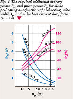
The definition of the required additional power for diode preheating is a subject of practical interest. The diode preheating power as a function of preheating pulse width pr and preheating duty factor Dpr is found based on the nonconstant temperature characteristics of the IMPATT diode. These characteristics define the transient heat resistance RT ( pr , Dpr ) vs. Dpr , pr and also diode geometry parameters.3 Numerical results discussed in this article are obtained for a double drift Si IMPATT diode with optimum doping profile at 8 mm wavelength with a p-n junction diameter dpn = 160 µm in the range of ambient temperatures of 60º to +70ºC and the semiconductor junction maximum temperature at the leading edge of pulse bias current 0 = 70º. The preheating current pulse adjoins the diode bias current pulse directly.
The results of calculations are shown in Figure 4 . The average Pav (solid curves) and pulse Pp (dotted curves) preheating power vs. duty factor D1 = 1 /T1 of pulses during the packets are presented for the pulse width values pr = 0.1, 0.3, 0.5 µs. It is seen that the average consumed preheating power decreases essentially if the preheating current pulse width decreases but, simultaneously, the amplitude of preheating current increases. This factor restricts the minimum value of pr because the preheating current amplitude should be less than the starting diode bias current of self-excitation. The principles of diode junction temperature stabilization presented here provide a decrease in the power consumption in comparison with methods of diode heat sink temperature stabilization.
THE ATTAINABLE RF PARAMETER STABILITY OF PULSED INJECTION-LOCKED IMPATT OSCILLATORS
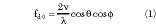
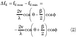
According to the equivalent linearization method,4 when condition D Yd /Yd << 1 is fulfilled, the relations that define the change in module D and phase D  of the complex reflection coefficient G 0 exp(jY0 ) at the oscillator terminals may be written as
where
D Um /Um0 = relative change in voltage amplitude
D  = phase change of complex function
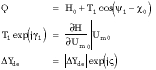
H = |H0 |exp(j 0 ) = d (w 0 ,Um , 0 ,I0 ) + 0 ( w 0 ), which are caused by changing the junction temperature and pulse bias current and I0 , respectively
The values D Um and D are defined by


where
Is = (8 Ps G0 )0.5
= locking current amplitude
Ps = level of input locking power
G0 = Y0
= load conductance at oscillator terminals
It is seen from Equations 1 to 5 that RF parameter variations of pulsed injection-locked oscillators depend essentially on the relationships between angles  which define phases of vectors H, T0 and Yd . These angles vary over a wide range when the input locking signal frequency fs changes. At the frequencies w º at which Q values are minimum, the regions of maximum instabilities appear inside the locking band. This peculiarity should be taken into account in designing highly stabilized injection-locked oscillators with a wide locking bandwidth. The attainable stability of the RF parameters over the locking bandwidth of a pulsed injection-locked IMPATT oscillator may be defined based on the presented equations.
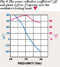
Numerical results for dynamic and stabilized performance presented here are determined for an IMPATT oscillator in the 8 mm wave range using a waveguide-to-coaxial microwave system. The resonant transformation of the diode junction impedance is fulfilled with the use of mounting and contact elements of the diode package. The resonant transformation solves the problem of diode and load impedance matching at high values of circuit efficiency. The simplified equivalent oscillator microwave circuit5 is shown in Figure 5 . The following parameters values (close to those of the realized oscillator sample) were used in the calculations: the diameter of the p-n junction dp,n = 160 µm, L1 = 0.1 nH, C1 = 0.27 pF, G0 n2 = 0.01 S, W0c = 50 W , rap = 20 W , rs = 0.5 W and X2 = X3 = X4 = 0; rap is an antiparasitic resistance placed in coaxial line; Xp is a reactance of a sliding back short in waveguide; Zd is an equivalent impedance of a packaged IMPATT diode; the diode bias current density J0 = 16 kA/cm2 at semiconductor structure temperature T 0 = 500 K; and the power of input locking signal Ps = 0.3 W. The power reflection coefficient G 0 2 (f) and phase 0 (f) vs. frequency over the locking bandwidth of the oscillator are shown in Figure 6 . Figure 7 shows the attainable variations of phase D (f) and power D P/P (f) for the temperature change interval of 390 to 500 K using the current compensation method. In the temperature range of 500 to 590 K, the attainable variations decrease by a factor of 6 to 7 times compared with results shown for the current compensation method. From the numerical results presented it can be seen that the phase instability D < 10º and the power instability D P/P =5 percent within the operating frequency band D f = 1.4 GHz when the initial temperature at current pulse leading edge is set to 0 = 390 K. The full locking bandwidth D fs = 2 GHz; near the low frequency limit of the locking band the instabilities increase and D max and D Pmax occur at the region where Q is minimum. The presented results correspond to the introduction of semiconductor junction preheating when the initial temperature is 390 K. The instabilities increase essentially without preheating and when the initial temperature of a diode 0 < 390 K.


CONCLUSION
The use of current compensation of the diode admittance change with temperature during the pulse width jointly with pulse preheating of the semiconductor junction for stabilization of the initial junction temperature at the leading edge of bias current pulses solves the problem of designing pulse power injection-locked IMPATT oscillators with high stability of amplitude and phase of the output signal over the wide range of ambient temperatures and a wide operating frequency band. The proposed principles of the preheating system provide diode junction temperature stabilization over the wide ambient temperature range at a high changing rate of factors affecting the diode temperature. The unique feature of the described method is the diode junction temperature stabilization without temperature stabilization of the diode heat sink or the microwave oscillator body. As a result, the high pulse rate of the pulse preheating system is achieved with a minimum of additional power consumption for stabilization of the diode junction temperature. *
References
1. T.T. Fong and H.J. Kuno, "Millimeter-wave Pulsed IMPATT Sources," IEEE Transactions on Microwave Theory and Techniques , Vol. MTT-227, No. 5, 1979, pp. 492499.
2. R.L. Eisenhart and R.S. Robertson, "Controlled Bias Preheating for Variable Duty Factor IMPATT Transmitter." IEEE MTT-S Microwave Symposium Digest , 1985, pp. 529530.
3. L.V. Kasatkin, "Solid-state Pulse IMPATT-diode Millimeter-wave Transmitters," Electronic Techniques , Series 1, RF Technique, Moscow, Russia, 1996, No. 2, pp. 4147.
4. Blaquiere Austin, Nonlinear System Analysis , Academic Press, New York, NY, 1966, p. 400.
5. L.V. Kasatkin and A.V. Gorbachov, "The Equivalent Replacing Schemes for Microwave Circuit of Solid-state Stabilotron Power Combiners," Electronic Techniques , Series 1, RF Electronics, Moscow, USSR, 1989, No. 9, pp. 5055.
L.V. Kasatkin is a leading scientist at the Science Research Institute "Orion" in Kiev, Ukraine. He received his scientific degree in the USSR in 1958 and became a doctor of technical science in 1990 when the subject of his thesis was "The Design Principles of Frequency Stabilized IMPATT-Diode Oscillators." His principal interests and work are in the fields of power vacuum and solid-state microwave devices. He may be reached via e-mail at al-kas@carrier.kiev.ua and by regular mail at PO Box N 565, Kiev, Ukraine, 03150
N.F. Karushkin is a chief engineer at the Science Research Institute "Orion" in Kiev, Ukraine. He received his scientific degree in the USSR in 1979, and the subject of his thesis was "The Microwave Semiconductor Control and Commuting Devices." His interests and work are in the fields of microwave semiconductor diode technology and the creation of active and passive microwave devices. He may be reached via fax at 380-44-446-52-91 and by regular mail at Balzak St. 86, Apt. 93, Kiev, Ukraine, 02232.