
Applying Switched Gain Stage Concepts to Improve Efficiency and Linearity for Mobile CDMA Power Amplification
Efficiency and linearity of the power amplifier contained in second-generation (2G) CDMA cellular mobile radios are critical parameters. Further system application of power control where the mobile unit transmits output power levels ranging from maximum to tens of decibels in back-off emphasizes the importance of optimizing the efficiency/linearity trade-off over a wide output power range to extend battery life of the radio. This article discusses improvements obtained using a switched gain stage power amplifier where the second stage (of a two-stage power amplifier) is bypassed at lower output power levels, thereby substantially improving performance in power back-off operation. Improvements in efficiency and battery lifetime are calculated with performance compared to traditional single-ended operation.
J. Staudinger
Motorola, Semiconductor Products Sector
Tempe, AZ
Present 2G CDMA-based cellular systems have adopted offset quadrature phase-shift keying (OQPSK) modulation for the reverse (mobile) link.1 The selection of this modulation format along with necessary spectrally limiting base band filters results in a waveform that exhibits both amplitude and phase modulation. This format necessitates the use of linear power amplification in the transmitter of the mobile unit to preserve amplitude and phase integrity of the signal.
Power amplifiers exhibit an inherent trade-off between linearity and efficiency. Efficiency (ratio of RF to DC power) increases with increasing signal level with a maximum occurring at signal levels that drive the amplifier in or near gain compression. As previously noted, a CDMA signal exhibits amplitude modulation. Thus, operating the amplifier at signal levels near gain compression inherently compresses peak envelope excursions and leads to an increase in distortion and adjacent-channel power ratio (ACPR). In addition to exhibiting nonconstant amplitude, a CDMA signal is phase modulated and variations in the amplifier's insertion phase with signal level (AM-to-PM conversion or phase distortion) contribute to an increase in ACPR as well. In general, AM-to-PM effects tend to be most significant for signal levels near gain compression. Hence, it is difficult to maintain acceptable linearity when amplifying a CDMA signal at levels where envelope excursions extend in or near gain compression of the amplifier. Some level of back-off is therefore required to limit compression, and a corresponding loss in afficiency is inherent.
A further aspect of 2G CDMA cellular systems affecting handset power amplifier performance is the application of system level power control. Power transmitted by the mobile unit can be adjusted on a periodic basis to combat environmental effects such as distance and multipath fading and to be consistent with link margin and base unit receiver criteria where all signals are similar in strength. Over a long-term basis of many data symbols, the handset power amplifier functions to produce average output power levels ranging from a maximum to power levels of perhaps tens of decibels in back-off. As noted previously, amplifier efficiency drops as the signal level is reduced; therefore, efficiency at reduced average power levels can be particularly important.
AMPLIFIER PERFORMANCE WITH A CDMA OQPSK SIGNAL
It is useful to consider several aspects in amplifying a CDMA-compliant OQPSK signal in context to the class or mode of amplifier operation. Namely, the average efficiency of the amplifier when driven by a nonconstant envelope signal and, secondly, the reduction in efficiency resulting when the amplifier operates in back-off as the average power level is reduced.
An IS-95-compliant CDMA modulated signal is generally considered narrowband and, as such, can be described in terms of a carrier with amplitude and phase components taking the form
v(t) = E(t) cos(w0 t + (t)) (1)
where w 0 defines the carrier frequency. The terms E(t) and f(t) describe amplitude (envelope) and phase modulation characteristics of the signal, respectively. Due to the baseband filtering applied to confine spectral energy along with OQPSK modulation, the signal envelope E(t) varies with time. Although dependent on the precise data used to construct the waveform and other factors such as the particular Walsh code used in the spreading sequence, a peak-to-average power ratio of approximately 5 dB is generally assumed (where Erms is the RMS value of E(t)).
In most types of amplifiers, particulalrly single-ended class-A and -B operation driven by an unmodulated sinusoid, efficiency is a function of signal or power level. In the case of a narrowband modulated CDMA signal, an instantaneous efficiency can be considered, which is proportional to the level of the envelope. Since the envelope E(t) is time varying, efficiency varies with the magnitude of the envelope and thus is time varying as well. It is customary to consider an average efficiency defined as the ratio of average RF output power (Pout_avg ) to DC power supplied from the battery (Pin_avg ) given by

For class-A and -B operation, efficiency is readily estimated when the active device is represented as a constant transconductance with accompanying tuned output networks.4 Neglecting voltage saturation effects, efficiency for rather idealized class-A and -B operation with single-tone (unmodulated) sinusoidal drive is proportional to Pout /Pout_max and (Pout /Pout_max )1/2 , respectively, as shown in Figure 1 , with maximum values of 50 percent and 78.5 percent under full drive conditions, respectively. The term Pout_max represents peak-envelope-power (PEP) occurring at a maximum signal level such that the amplifier is traversing full load line excursions. As the signal level and power are reduced (back-off), efficiency falls per the above relationships. For amplitude modulated signals, efficiency is lower since the maximum (50 percent for class A and 78.5 percent for class B) occurs only at time intervals when the envelope voltage is maximum (Emax ). For example, Figure 2 shows the envelope E(t) for a few data symbols of a CDMA signal and, thus, for envelope values less than Emax , efficiency is less than the described maximum values.


Class-A and -B average efficiency in amplifying a CDMA signal can be calculated based on techniques that consider the probability density function of envelope voltage.4 Alternatively, a direct calculation is applied. First, a representative OQPSK signal based on a pseudorandom noise (PN) data sequence with appropriate baseband filtering and Walsh code spreading is generated. The average RF power in the signal is proportional to the RMS envelope voltage squared (Erms 2 ). The input power supplied from the battery varies with the magnitude of the envelope (and thus time). As noted, at a given envelope level, efficiency is proportional to (E/Vdd )2 and E/Vdd , for class-A and -B amplification, respectively (where Vdd is the battery voltage). Hence, input power (at a given envelope level) is the ratio of E2 to (E/ Vdd )2 (class A) or E2 to E/ Vdd (class B). The DC value or average input power of interest in Equation 2 is then obtained by direct calculation.
Two conditions are of particular interest. Consider first full drive conditions where the class-A and -B amplifiers function at maximum average output power such that full load line excursions occur at maximum envelope voltages Emax . Application of Equation 2 suggests class-A and -B amplification results in average efficiencies of 18 and 48 percent, respectively. A second situation of interest is power back-off where the average level of the signal is reduced such that peak envelope voltages do not result in full load line excursions. The average efficiency for class-A and -B amplification degrades as shown in Figure 3 .

CDMA TRANSMITTED POWER PROFILE
In addition to short-term envelope variations, IS-95 systems make adjustments in mobile unit transmitted power over relatively long time intervals equivalent to many data symbols (for example, 1.25 ms). Figure 4 shows one possible probability distribution function (PDF, p(Pout )) of average amplifier output power (long term) in a CDMA reverse link urban environment based upon measurements. It is observed that radio transmission at a maximum average amplifier output power of ~ 0.7 W is statistically very low. The most probable output power level is on the order of a few milliwatts. The data shown here are similar to those reported by others and illustrate that near maximum output power amplifier operation is very limited.2,3

Given the statistical long-term nature in average transmitted power levels, it is appropriate to define several quantities to gauge the effectiveness of the amplifier for this environment. Principally, the average RF output power from the amplifier is defined by
The average current supplied by the battery is
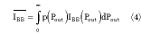
The average power supplied by the battery into the amplifier is given by

Borrowing from the work of Hannington et. al.2 average power-usage efficiency is given by
The quantity *usage accounts for amplifier efficiency variations over long time intervals and as such is a useful figure of merit in quantifying effective amplifier efficiency for this environment.
LINEARITY
In addition to efficiency, amplifier linearity is a critical performance element of the system. The OQPSK reverse-channel signal exhibits time-varying amplitude and phase variations that must be maintained by the amplifier. Gain compression/expansion and/or phase distortion effects produced by the amplifier alter these characteristics and lead to signal distortion and spectral regrowth. Adjacent- and alternate-channel power ratios (ACPR) are used to quantify regrowth. The adjacent-channel power ratio (upper and lower channels) is defined as the ratio of power in a 30 kHz bandwidth offset from the carrier by 885 kHz to the power in the main CDMA channel. The alternate- channel power ratio is defined similarly except that alternate-channel power is measured in a 30 kHz bandwidth offset from the carrier by 1.98 MHz.
SWITCHED STAGE RF POWER AMPLIFICATION
A generalized class-A/B two-stage FET-based RF power amplifier topology is shown in Figure 5 . Input-, interstage- and output-matching networks are denoted as M1, M2 and M3, respectively. In general, the design of the linear power amplifier must be consistent to deliver the maximum required output power at a desired level of spectral linearity given the CDMA input modulated stimulus. Hence, device sizing of Q1 and Q2, first- and second-stage load lines (G1 ,G2 ), and quiescent drain bias are major design elements.

In power back-off where output power is reduced, the ratio of DC to RF power decreases and, hence, efficiency drops as previously illustrated. For a two-stage amplifier, both Q1 and Q2 are then functioning at a point where the RF signal is traversing a small excursion on the respective Q1/Q2 load lines. Considering the PDF illustrated in the example, at highest probability of output power (more than 20 dB in back-off) an idealized class-B amplifier is less than five percent efficient. In class-A operation, efficiency drops well below one percent.
Fundamentally, efficiency can be raised at reduced power levels by requiring the RF voltage excursion to occupy a larger portion of the device's load line. One method to accomplish this is by applying switched gain stage concepts. For example, consider the topology shown in Figure 6 where the second stage can be bypassed. At low to moderate output power levels, all signal amplification can be achieved with Q1 and then the RF signal is routed from the first stage to the output (bypass mode). At higher power levels, the amplifier operates with both gain stages. The larger Q2 device and its load line supports the increased signal level. In power back-off, efficiency is potentially improved using the bypass operating mode. The improvement results from adjusting VG2 such that Idd2 is zero, and possibly setting the Q1 load line (G1bypass ) to a more appropriate value than required in the nonbypassed mode. In general, G1 exhibits two discrete values depending on whether it is driving Q2 or bypassing Q2.

A number of circuit architectures with varying levels of complexity are possible for realizing a switched gain stage amplifier. A few possibilities are shown in Figure 7 . Many choices are possible with respect to placement of the RF switches. They can be placed either prior to, after or integrated with interstage and output matching structures. Nonetheless, compared to nonswitched gain stage amplifiers, additional components are required. Generally, RF switches are needed to bypass Q2 and, possibly, additional matching circuitry is required to implement the desired Q1 load line in the bypassed mode.

The success of realizing this architecture rests in minimizing losses associated with the switches and in partitioning the interstage/output matching elements/topology with the switching elements to reduce losses and circuit size. Size constraints that favor integrating the switches and matching structures must be balanced against the topology and the inherently higher losses of on-chip inductors vs. off-chip components. Additionally, circuit topology and performance trade-offs must be carefully balanced against cost goals for the solution to be viable in an extremely competitive handset market place.
RF PA EVALUATION AND MEASUREMENTS
A prototype RF switched stage power amplifier was designed using AlGaAs/InGaAs heterostructure insulated-gate FET technology. The selected device technology eliminates any need for negative bias voltages and allows for supply voltage operation for both active devices and RF switches.57 A key feature of the device technology is a high Schottky turn-on voltage, VTO = +1.8 V at 1 mA/mm, which reduces gate current under high RF drive levels and also improves power density due to the large VTO VTH difference.
The amplifier was designed with the intent of maximizing the efficiency/linearity trade-off with respect to the power profile previously shown. Measured amplifier performance using an IS-95 CDMA-modulated stimulus at 835 MHz with a 3.5 V battery is shown in Figure 8 . In the bypass mode, RF switching routes the signal from the first stage to the output. A desired value for Q1 load is also switched in to improve efficiency/power performance. Output power levels up to +18.5 dBm are supported with the amplifier exhibiting desired linearity of 46 and 56 dB adjacent and alternate ACPR, respectively. In deep power back-off, battery current drops dramatically from ~ 200 mA (full two-stage PA) to approximately 25 mA in the bypass mode. For power levels greater than +18.5 dBm, the amplifier functions with both Q1 and Q2. Power levels up to +29 dBm are achieved at the above noted linearity levels. A small-signal gain of 13 and 25 dB is obtained in the bypass and full operation modes, respectively.

Figure 9 shows amplifier efficiency with respect to the power profile. Selecting a mode switching point of +18.5 dBm allows the amplifier to function in the bypass mode most of the time. With the amplifier functioning at a switch point of +18.5 dBm, average efficiencies of 25.9 and 38.9 percent are achieved at power levels of +18.5 and 29 dBm, respectively.

Average usage efficiency is calculated by considering the probability density functions previously shown along with Equation 6. Results are listed in Table 1 assuming the amplifier switches modes at +18.5 dBm. For comparative purposes, average efficiency is also shown for this amplifier when operating in a nonswitched mode across the full output power PDF. An improvement in efficiency of greater than 4.5X is realized.

CONCLUSION
A switched output two-stage RF power amplifier has been demonstrated with application to 2G CDMA mobile handsets. Compared to the two-stage amplifier functioning in class-A/B operation over the full PDF power range, an improvement in average user efficiency of greater than 4.5X is realized with the switched mode architecture. *
References
1. TIA/EIA IS-95, "Mobile Station-Base Station Compatibility Standard for Dual-Mode Wideband Spread Spectrum Cellular System," Telecommunications Industry Association , July 1993.
2. G. Hanington, P. Chen, P. Asbeck and L. Larson, "High-efficiency Power Amplifier Using Dynamic Power-supply Voltage for CDMA Applications," IEEE Transactions on Microwave Theory and Techniques , Aug. 1999, pp. 14711476.
3. J.F. Sevic, "Statistical Characterization of RF-Power Amplifier Efficiency for CDMA Wireless Communication Systems," Wireless Communications Conference Proceedings , Boulder, CO, Aug. 1997, pp. 110113.
4. F. Raab, "High Efficiency Power Amplifiers," Short course notes, Green Mountain Radio Research, 1985.
5. E. Glass, J. Huang, M. Martinez, O. Hartin, W. Valentine, M. LaBelle and E. Lan, "A Single Supply Device Technology for Wireless Applications," GaAs IC Symposium Proceedings , 1999, pp. 123126.
6. E. Glass, J. Huang, J. Martinez, W. Peatman, O. Hartin, W. Valentine, M. LaBelle, J. Costa and K. Johnson, "A True Enhancement Mode Device Technology Suitable for Dual Mode Dual Band Power Amplifier Applications," IEEE MTT-S Symposium Proceedings , 1999, pp. 135138.
7. E. Glass, J. Huang, J. Staudinger, M. Shields, M. Martinez, O. Hartin, W. Valentine and E. Lan, "Application of Enhancement Mode FET Technology for Wireless Subscriber Transmit/Receive Circuits," Journal Solid State Circuits , Sept. 2000.
Joe Staudinger is a senior member of the technical staff at Motorola's semiconductor products sector. His work primarily involves large signal modeling of active devices, non-linear simulation and development of RF circuits with application to the wireless handset market. He is a senior member of the IEEE and holds 20 patents.