
Low Power Delay Filters for MCPA Applications
K&L Microwave Inc.
Salisbury, MD
Multicarrier power amplifiers (MCPA) and their importance to wide modulation have received extensive coverage in recent literature.1 The demand for faster data rates has given a boost to the MCPA industry and magnified interest in improving performance and reducing the size and cost of MCPA assemblies. In an MCPA assembly, shown in Figure 1, the delay elements represent an area of potential improvement. These elements, which exist in both paths, are responsible for balancing intermodulation (IM) product mitigation. In a deeper sense, minimizing delay differences between the paths widens the bandwidth over which the desired cancellation is achieved. A novel advance in the design of delay elements promises performance and manufacturing benefits.

In the past, coaxial transmission lines have been used for MCPA delay elements; however, other delay element realizations have begun to replace coaxial transmission lines in the primary and secondary loops for two distinct sets of reasons. In the primary path, delay follows RF amplification, and cavity filters are replacing coaxial cables because output power is an important consideration and cavity filters exhibit less loss. Insertion loss introduced by the delay element is more tolerable in the secondary loop, where the main objective is amplification of the IM products, and the delay element precedes the amplification stage.
Manufacturing issues and fine-tuning considerations for the entire MCPA assembly indicate a need to replace coaxial transmission lines in the secondary loop. With a typical air-filled structure, one foot of cable delays a group of signals by approximately one nanosecond. Frequently a cable averaging 10 to 15 feet in length is arranged in a spiral that must be carefully tacked down to the PCB or mounted on a spool. Spool mounting adds to the total height of the module. If connectors are used in production, the MCPA assembly becomes large, and fine-tuning requires the removal of connectors for small adjustments to the cable length. If connectors are not used, special care is required to ensure good grounding of cable jackets. Coaxial delay lines complicate assembly, frustrate automation attempts and increase repair costs over emerging alternatives.
For several decades, filters have been recognized as a viable alternative to coaxial transmission lines as delay elements, and special cross-coupled structures have been developed to flatten delay response. In the early days of satellite communication, delay filters were of the high QU cavity TEM or TE/TM waveguide types. While this time-honored approach is being successfully employed for delay filters in the main MCPA loop, it is not feasible as an alternative to coaxial elements in the secondary loop because of size. Only lumped element filters or distributed lines on high dielectric material can match the relatively small size of miniature coaxial cables. In these structures, inductors and patch capacitors radiate in a fashion that precludes cross coupling of resonators. Any attempt to control all coupling of lumped elements requires heavy channelization and lengthy tuning time. With lumped element filters, the degree of complexity strongly depends on the number of sections. For current applications, 6 to 12 cross-coupled resonators are required to achieve necessary delay levels -- a number of cross-couplings that is difficult to realize with lumped components.
NEW DESIGN
A new miniature delay filter has been developed. Instead of realizing the entire delay with a single filter structure, the required delay level is achieved by a combination of two structures, as shown in Figure 2, and the summation of their two delay responses: a parabolic shape and an inverse parabolic shape. In the passband, the delay pattern of a bandpass filter has a parabolic shape, with the minimum delay located in the center of the band (at the bottom of the parabola). By allowing the delay variation across the desired passband to be on the order of 1.5 ns, the 3 dB bandwidth of the filter is just slightly larger than the actual passband. The filter produces a good portion of the delay, operating in the narrowband sense. (Other designs broaden the filter's passband to achieve flatness, thereby requiring more sections to increase delay, since delay decreases as equal-ripple bandwidth increases.)

The compensating inverse parabolic shape is realized by a network composed of a 3 dB hybrid quadrature with two identical resonators loosely coupled to two of the four ports. This stage serves dual purposes. First, it produces the desired inverse parabola delay shape. Second, excessive delay, occurring at mid-band, creates excessive loss, which helps to flatten the insertion loss pattern of the narrowband filter. In short, the coupler and the resonators provide delay and amplitude equalization simultaneously.
Figure 3 shows the delay vs. frequency with C0 as a parameter and the unloaded Q factor, QU = 300. As C0 is decreased, the maximum delay level gets higher and the bandwidth becomes narrower where the resonance frequency increases.

As the signals enter the hybrid quadrature, they split equally in amplitude, but with a 90° phase difference, into the two loosely coupled ports. The reflection coefficient looking into the resonator represents an inverse parabola for the delay shape. Intuitively, because of the resonance effect, the frequencies around mid-band are delayed more than the frequencies at the band edges. Depending upon the quality factor of the lumped components, the frequencies at mid-band will always exhibit more loss than frequencies at the band edges. This is commonly observed as a straightforward relationship between delay and loss. Next, the two groups of signals are reflected back into the coupler. Since both coupled ports are identical, the signals are out of phase at the input port but add in-phase at the output port, leading to the bandpass filter.
A DESIGN EXAMPLE
A delay level of 18 ns across the 3G UMTS transmit band (2110 MHz to 2170 MHz) is required. The filter portion consists of seven sections with a 3 dB bandwidth of 118 MHz, a capacitor quality factor, QC = 1000, and inductor quality factor, QL = 180. The stand-alone filter's parameters are minimum insertion loss at mid-band of 4.85 dB and amplitude variation of 0.4 dB, minimum delay at mid-band of 12.6 ns and delay variation of 1 ns, and phase deviation from linearity of ±3.5°. (Note that this level of phase deviation is unsuitable for MCPA applications.)
Based on these parameters, it is easy to define the values of the inverse parabola to add to the filter's delay in order to achieve the required 18 ns. The inverse parabola contributed by the hybrid quadrature stage must provide about 5.5 ns at mid-band and 4.5 ns at the band edges. The new concept was first built in the form of a lumped element filter cascaded with the coupler stage, which was coupled with two lumped resonators. The new delay line filter in a surface-mount configuration measures only 1.5" x 0.5" x 0.3". The measured delay of the filter, shown in Figure 4, represents a minimum delay of 17.7 and 18.2 ns at the band edges. This delay is well within the specification limits of 18 ±0.5 ns.

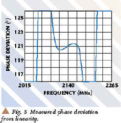
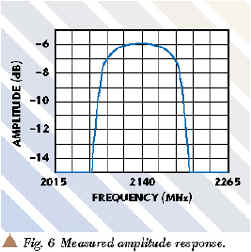
One of the most important parameters of the delay line filter is the phase deviation from linearity. The mitigation of IM products is strongly dependent upon this value, as extensively described in the literature.2 The measured deviation in this design example is less than ±0.5°, as shown in Figure 5. Phase deviation from linearity improved sevenfold over the value of the stand-alone filter, while the delay level increased from 13 to 18 ns. Figure 6 shows the measured amplitude response, which exhibits an amplitude variation of 0.12 dB across the transmit band, with a return loss level of better than 20 dB (not shown). The quadrature hybrid performs as a delay and amplitude equalizer, reducing the variation more than threefold.
CONCLUSION
A new topology for implementing delay line filters has been developed. Measured results are in excellent agreement with the theory. The new approach, for which international patent applications are pending, has many advantages for the design and manufacture of MCPA assemblies, including suitability for pick-and-place installation of the delay elements. Coaxial delay lines require manual installation. The new delay filters remove the final obstacle to full automation of the manufacture of MCPA assemblies. The new approach also displays better isolation between RF paths. Integration of the input splitter and couplers C1 , C2 and C3 into one assembly ensures that isolation is maintained between the RF paths, essential criteria for MCPA operation. This concept was built, tested and found to be superior in performance. In comparison with coaxial cables, the narrowband delay filter concept provides out-of-band emission rejection. In addition, the approach provides quick turnaround and high volume production capability. The new delay filters can be manufactured from lumped elements or in distributed (interdigital) form on high dielectric material. The distributed form is well suited for tape-and-reel applications. All couplers, splitters and delay elements on the secondary path could potentially be designed and realized on high dielectric material (er = 25), thus eliminating assembly and tuning time and resulting in cost reductions. For further information, contact Rafi Hershtig at rhershtig@klmicrowave.com or Brian Wixon at bwixon@klmicrowave.com.
References
1. Barney Arntz, "Second Order Effects in Feedforward Amplifiers," Applied Microwave & Wireless, January 2000.
2. Nick Pothecary, Feedforward Linear Power Amplifier, Artech House, 1999.
K&L Microwave Inc.,
Salisbury, MD
(410) 749-2424.
Circle No. 301