
A 20 GHz low phase noise voltage-controlled oscillator (VCO) uses InGaP GaAs heterojunction bipolar transistor (HBT) technology. A push-push negative gm VCO configuration taking its output signal from a capacitive base common node of the cross-coupled transistors is employed to achieve a high oscillation frequency and low phase noise. The VCO oscillates from 19.44 to 20.04 GHz. Measured phase noise is -111.8 dBc/Hz at 1 MHz offset from a 19.78 GHz carrier. It consumes 31 mW from a 5 V supply and occupies an area of 0.514 mm × 0.622 mm. Its figure of merit is -182.8 dBc/Hz.
The increased demand for high data-rate wireless communication is driving the development of RFIC to higher frequency bands. For high frequency RFICs, InGaP GaAs HBT technology is a good candidate. Compared with CMOS, InGaP GaAs HBTs have the advantages of potentially higher fT, higher transconductance and lower 1/f noise. In addition, InGaP GaAs HBTs have been shown to have inherent radiation hardening, making them well suited for the applications in the space environment.1-2
In transceiver systems, VCOs are key components, and most systems require low phase noise and jitter, which degrade system performance by reducing accuracy and increasing errors. At RF frequencies, two VCO topologies (cross-coupled3-6 and Colpitts7-10) are widely used. From Andreani et al.,11 it can be concluded that both topologies are capable of very good phase noise; however, it also has shown that a cross-coupled VCO can achieve lower phase noise than a Colpitts.
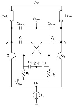
Figure 1 Negative gm differential VCO.
In order to extend the output frequency range, a frequency doubler combined with a VCO may be used, but this increases circuit complexity and power consumption. An alternative is the so called push-push oscillator,12-13 which extracts the second harmonic of the VCO core. In this type of oscillator, the desired frequency tuning range is twice that of the VCO core and there is potentially less power consumption. Depending on the node from which the second harmonic is extracted, three architectures are found in the literature. The extracting node can be the collector common node,14 base common node13 or the emitter common node.15 Compared with the collector common node and emitter common node, the base common node is most efficient at extracting all the available second harmonic from the tank.13 In this article, we describe a 20 GHz push-push negative gm VCO that takes its output signal from a capacitive base common node of the cross-coupled transistors.
CIRCUIT DESIGN
Architecture
The circuit schematic of a conventional negative gm differential oscillator is shown in Figure 1. The cross-coupled transistors (Q1 and Q2) generate a negative gm to overcome tank loss. The capacitive voltage divider, composed of C1 and C2 + CBE (CBE is the base-emitter junction capacitor of Q1), is designed to attain an approximate loop gain of three in order to maximize the tank swing and simultaneously optimize signal amplitudes at the base nodes to feed back from the collectors of Q1. It is known that phase noise degrades rapidly if the base-voltage swing becomes larger than a certain optimum value since Q1 enters deep saturation.16
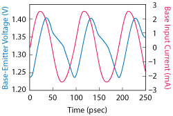
Figure 2 Base-emitter voltage and base current waveforms.
The common node (CN) of the capacitive voltage divider can be regarded as a virtual ground for the fundamental frequency (ωo) just like the emitter common node (EN), but that CN could be a very effective summing node for the second harmonics (2ωo) of the fundamental signals (V+, V-) of the VCO core. Note that the CN can be regarded as a base common node compared with the conventional emitter or collector common node. The advantage of using the CN for output extraction is that it does not require any additional circuitry such as frequency doubler to create 2ωo, other than the conventional negative gm oscillator circuit, and does not reduce the common-mode impedance at node EN. It has been reported that an additional inductance inserted between node EN and the tail current source Io can increase the common-mode impedance and the signal swing at node EN, but it is at the cost of an additional bulky inductor.
Operating Principle
The mechanisms responsible for second harmonic generation at the VCO core are investigated to understand circuit operation. A simple 20 GHz VCO is designed based on the circuit schematic of Figure 1 with a 10 GHz LC tank. The first is the nonlinear switching characteristics of the base-emitter junction diode. Although the circuit operates nonlinearly, it is helpful to use linear circuit analysis when appropriate.
Figure 2 illustrates the simulated waveforms of the base-emitter voltage (VBE) and the base input current (IB) of Q1. The base current leads the base-emitter voltage by 90 degrees due to the base input capacitance, and the upper half period of VBE is distorted compared with the undistorted sinusoidal waveform. The distortion is due to the exponential current-voltage relationship of the base-emitter junction diode given by
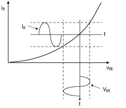
Figure 3 Base-emitter voltage waveform distortion.
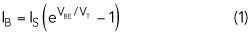
where Is is the saturation current and VT is the thermal voltage. Figure 3 illustrates conceptually how the upper half period of VBE is distorted by voltage clipping when the base current is a large sinusoidal signal.
The second cause for second harmonic generation is the different time constants involved in charging and discharging the base-emitter junctions in the circuit. Again, a linear circuit analysis provides an intuitive understanding. The time constant at the base-emitter nodes is given by
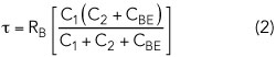
where RB is the base input resistance. As shown in Figure 4, in region I, IB is high, i.e., RB is small, so that the corresponding τ is small. This results in a fast rise time. The inverse occurs in region II.
Figure 4 Rise and fall times of the base-emitter voltage vs. τ.
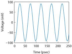
Figure 5 Voltage at the capacitive common node (CN).
These two mechanisms, together, contribute to second harmonic generation in the base-voltage waveform. When they are summed at the capacitive CN, the fundamental components at ωo cancel out due to their 180 degree phase difference and only the second harmonic components add constructively. This results in 2ωo at the output as shown in Figure 5. Moreover, the amplitude of the voltage waveform at the capacitive CN is not divided down by the capacitive divider. By contrast, the differential-mode fundamental signals V+ and V- are reduced by the same capacitive divider. Therefore, the CN node is capable of extracting all the available second harmonic components very efficiently from the tank.13
MEASUREMENT RESULTS
The technology used in this work is the InGaP GaAs HBT process from WIN Semiconductors Corporation. The process offers four types of NPN transistors, Q1H051B1, Q1H101B1, Q1H151B1 and Q1H201B1, with different emitter lengths (5, 10, 15 and 20 μm, respectively). Main electrical properties for NPN transistors are the collector-emitter breakdown voltage BVCEO = 9 V, the maximum unity current gain frequency fT = 65 GHz and the maximum unity power gain frequency fmax = 80 GHz. Passive components, including two metal layers, two types of capacitors, resistors, varactor diodes and inductances, as well as back side via holes are available in the process. Passive and active device models have been implemented and validated by simulation with Keysight Advanced Design System (ADS) software.