
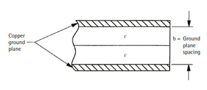
Figure 11 Stripline Evolution, coaxial cross-section
(a) to stripline cross-section (b).
Stripline is of uniform construction. Figure 9 depicts that uniformity, with the circuit being completely surrounded by dielectric on all sides. Because of that uniformity, stripline has a natural shielding effect on the circuit because it is completely enclosed, with metal on top and bottom. A stripline package also has metal on the ends and sides, resulting in a circuit within a complete metal box with excellent shielding.
An important parameter in stripline is the ground-plane spacing (GPS), shown in Figure 11. GPS is, as the name implies, is the spacing between the inner surfaces of the ground planes, designated as b. It is used to calculate the width of transmission lines (w) that are etched on the circuit board and the spacing (s) between two transmission lines. The relationships between w, s and b are shown in Figure 12.
A close tolerance on circuit board dielectric thickness must be maintained to ensure that the widths and the spacings are as accurate as possible. Consider that the characteristic impedance of a strip transmission line is determined by the ratio w/b; and similarly, the coupling of energy between two transmission lines is determined by the s/b ratio. If the b dimension in the denominator is not tightly controlled it is difficult to maintain a desired characteristic impedance as well as a desired level energy coupling between circuits.
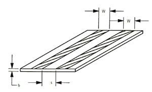
Figure 12 Ground plane spacing.
Stripline has become a popular medium for the construction of transmission lines and microwave circuit components. A drawback to using stripline for some applications is also touted as an advantage; it is a sealed enclosed structure. Although it offers good circuit shielding, there is limited access to circuit elements for test and troubleshooting. Because stripline packages contain laminated boards laminated boards and are often epoxy sealed, semiconductor devices such as diodes and transistors are generally not integrated into the structure, unless the integrated module is considered non-repairable.
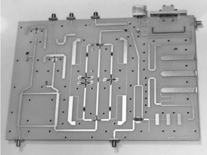
Figure 13 Relationships of ground plane spacing (b), transmission line width (w), and spacing between lines (s).
For many applications, stripline is an excellent choice as a high frequency transmission line. Where there is a requirement for excellent shielding, strip transmission line should be considered. Also, stripline is popular for the construction of passive components, such as couplers, power dividers, filters and impedance transformers. Figure 13 shows a stripline circuit with the top dielectric and ground layers removed to show the center conductor patterns that form the components.
Microstrip
Microstrip transmission line solves the problem of inaccessibility that stripline poses. Microstrip, shown in Figure 14, is similar to stripline, except that there is no top dielectric or conductor layer. There is nothing but air on top of the circuitry and a dielectric material underneath with a bottom ground plane. The width of the transmission line is designated by w, t is the thickness of the copper circuit and b is the thickness of the dielectric. It can be seen that b is similar to that for stripline except that it represents only one thickness of material.
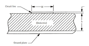
Figure 14 Stripline with the top dielectric and ground layers removed to expose circuit elements.
The material thickness of microstrip is as important as it is for stripline, and the relationships are similar. What is different in microstrip, however, is the dielectric constant. In stripline, the dielectric surrounding the center conductor is uniform. Stripline due to its symmetry is well-behaved. Microstrip, while it has a uniform dielectric material underneath its circuit element, has only air above it. The boundary between the dielectric material and the air has been the subject of numerous research projects and papers. The interface can be simplified if one assumes the existence of an effective dielectric constant, εeff, the resultant of the two dielectric constants (air above and the dielectric material below). The calculation takes into account the relative dielectric constant of the material, εr, and the dielectric constant of air, εo = 1.
The effective dielectric constant is used for all calculations where a dielectric constant term is used. Note that every time the impedance of a microstrip line changes, the effective dielectric constant changes as well. That is because the microstrip width changes with a change in impedance. The lower the impedance, the wider the line and vice versa. To calculate a filling factor for microstrip, which is a compensating factor for the difference in dielectric constant, the ratio w/b ratio is used. Thus, a change in impedance is a change in filling factor and, consequently, a change in effective dielectric constant. The relationship between impedance and effective dielectric constant is a point that sometimes escapes designers. This relationship must be taken into account many times in the design of a multisection power divider or directional coupler. Such devices require different impedance lines that are all one quarter-wavelength long.
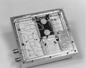
Figure 15 Microstrip transmision line.
Microstrip transmission lines are probably the most common types of transmission lines found in today’s RF and microwave circuits. The wireless markets use many microstrip circuits that enable easy component placement and attachment on top of the circuit board. Manufacturers that use surface mount technology (SMT) components use microstrip because of the ease of construction. It is clearly easier to attach components to a circuit board that has all the transmission lines on top of the board and very visible (see Figure 15).