
Remtec Inc. has commercialized etchable gold thick film process for High Definition Thick Film (HDTF) circuitry as a low-cost alternative to thin films. Remtec’s new offering represents a significant advancement in miniaturization, circuit density and performance.
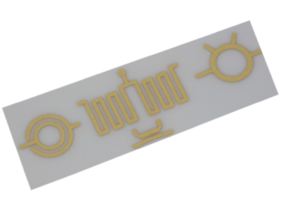
Remtec’s new etchable gold substrates allow the use of ultra-fine lines with a standard line/spacing resolution of 50/50 μm (0.002 in.) and premium circuit of 25/25 μm (0.001 in.). Circuit designers can also benefit from Remtec’s capability for added value features available on the same substrate. In addition to an etchable gold circuit, Remtec’s HDTF can incorporate conductor multilayers. It also integrates built-in components such as Lang couplers, inductors, filters and high precision resistors in a wide range from 50 mΩ to 1 MΩ laser trimmed to ±1 percent on the same ceramic base.
Remtec supports the new line of advanced HDTF substrates with new, state-of-the-art processing equipment in a class 1000 clean room. Design engineers can also take advantage of Remtec’s well-known core competency technologies such as AgENIG® (Electroless Nickel Immersion Gold on Silver) and PCTF® (Plated Copper on Thick Films) metallization in their ceramic package designs.
Typical applications of Remtec’s etchable gold HDTF ceramic metallization are for products requiring high circuit density and conductor proximity. HDTF substrates used for high performance products such as mmWave microwave circuits and high pin count analog and digital designs. They are ideal for radar, missile and SATCOM systems in both defense and industrial applications.