
CLOCK RECOVERY AT GIGABIT-PER-SECOND DATA RATES
Abstract:
Many devices used in high speed optical fiber terminal equipment are microwave electronic circuits. One such device is an electrical clock recovery circuit. Since bit rates of data signals in optical communications exceed 1 Gbps, the clock recovery technique becomes a very specific problem. This article is a review of electrical clock recovery techniques in optical communications.
Gigabit-per-second data rates are usually related to optical communications since other communication channels cannot transfer such high data rates. Optical communications started approximately 30 years ago with the invention of low loss optical fiber. The main advantages of optical fiber in comparison to other communication mediums are very low attenuation (0.2 dB/km) at a typical operational wavelength of 1.55 μm and a very large bandwidth (several terahertz).

Fig. 1 A single optical channel transmitter and receiver.
A single optical channel point-to-point terahertz transmitter and receiver are shown in Figure 1. Single optical channel refers to one optical carrier modulated by several electrical channels. The capacity of an optical-fiber link can be further increased by a wavelength division multiplexing technique where several optical carriers at different wavelengths are modulated by electrical channels.
An optical transmitter consists of an electrical multiplexer, scrambler, electrical amplifiers, laser diode and external optical modulator. The laser diode is modulated by an electrical multiplexed data signal. The modulated signal is sent through the optical fiber and detected by a PIN photodiode. The detected data signal is then amplified, regenerated, descrambled and demultiplexed.
The presented optical link consists of optical and electrical devices. The transmission takes place in the optical domain while the modulating signal and detected signal are electrical signals. Data rates of single-channel optical links available commercially today are 10 Gbps, while 40 to 80 Gbps single-channel systems are being developed.

Fig. 2 Spectra of the (a) NRZ and (b) RZ data signals.
At first glance, it seems that hybrid optical and electrical systems are not the most practical. Therefore, the research in optical communications is focused on building all-optical links and networks since optical devices should, in principle, process much higher bandwidths than electrical devices. However, the technology of all-optical devices is expensive in comparison to electrical equivalents and usually shows poorer performance and less compact implementation. Of course this situation can be changed in the future. On the other hand, the weakness of the electrical devices are lower bandwidths and cumbersome optical-to-electrical conversion, which must be performed at certain points in optical networks (for example routers where routing is done electrically). However, the technology of optical and electrical devices is improving and the bandwidths of electrical devices should reach 80 or even 160 Gbps in the future. The consequence is that every optical communication link still needs microwave circuits for its operation. As the bandwidths in optical communications are the largest bandwidths possible they also present a challenge for microwave engineers.
DATA FORMATS IN OPTICS
Several different electrical circuits are used in optical links; one of them is the clock recovery circuit. The purpose of the clock recovery circuit is to extract the clock signal out of the data signal in the receiver. The extracted clock is then used to detect the optimal sampling points in the data signal. Therefore, the extracted clock must be synchronized in frequency and in phase with the data signal.
The principle of operation of the clock recovery circuit depends strongly on the coding used in the data signal. A large number of pulse shapes and codes can be used in digital communications, but only two types of coding are widely used in optical communications: non-return-to-zero (NRZ) and return-to-zero (RZ).
It is important to understand that modulators in optical communications modulate the optical power. Since negative power doesn't exist the modulating data signal consists of positive pulses representing logical ones and pulses of no amplitude at all representing logical zeros. NRZ and RZ data signals and their power spectra are shown in Figure 2.
NRZ coding uses square pulses, which last the entire bit period. On the contrary, RZ uses square pulses that last less than the entire bit period. Obviously, the NRZ data signal has a narrower bandwidth and provides better spectral efficiency than the RZ signal. Because of the limited frequency response of electrical devices NRZ signals present the most suitable coding to be processed by electronics. One of the disadvantages of the NRZ signal, seen from its power spectrum, is the lack of a discrete spectral line at the clock frequency (f = 1/T), which makes the clock recovery more difficult.
To explain the advantages of the RZ signal compared to the NRZ signal, the properties of the optical fiber must be discussed. The attenuation of the fiber depends on the wavelength of the transmitted signal. The lowest attenuation achieves the value of 0.2 dB/km at the 1.55 μm wavelength. Therefore, the spectral band around the 1.55 μm wavelength is mainly used for transmission.
The optical fiber is a dispersive and nonlinear transmission line affecting the transmitted signal. In dispersive transmission lines, different wavelengths (or frequencies) travel with different velocities, resulting in broadening of the transmitted pulse in the time domain. At the same time, an optical fiber is also a nonlinear transmission line: The refractive index depends on the power of the transmitted signal. One of the consequences is self-phase modulation of the signal because the power and consequently refractive index vary along the pulse. The effect of the nonlinearity depends on the power of the transmitted signal.
Nonlinearity controlled by the pulse power can lead to partial or complete cancellation of the dispersion in the pulse. In fact, the pulse shape in which the cancellation completely occurs is called a soliton. It is not within the scope of this article to explain how this cancellation occurs. (More information on this topic is published in Kazovsky, et al.8)
If the data signal consists of pulses of equal duration and equal power, then all the pulses broaden by the same rate when travelling through the fiber. This scenario is true for the RZ coding. The special case of RZ coding where the pulses are resistant to dispersion is called the soliton transmission.
In the NRZ, coding pulses are not the same length because two sequences of a different number of ones represent two pulses of different length. Consequently, the pulses in the case of NRZ transmission do not have the same length and, therefore, are affected by the dispersion in a different way.
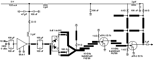
Fig. 3 The nonlinear microstrip circuit
Fig. 4 The NRZ clock recovery circuit's block diagram with eye diagrams of the processed signals.

The main advantage of the RZ signal is that it can be more resistant to dispersion than a NRZ signal if the correct power of the optical pulses is chosen. A side advantage is the presence of a discrete spectral line in the spectrum at the clock frequency, which makes the clock extraction easier. The obvious disadvantage is poor spectral efficiency because of the relatively large bandwidth.
CLOCK RECOVERY
At Gbps data rates the most widely used technique for clock recovery is the spectral line method.2-7 The basic purpose of this method is to locate a discrete spectral line in the spectrum of the received data signal and extract it with a narrow bandpass filter. The lack of discrete spectral lines in the NRZ signal spectrum makes the clock recovery for the NRZ signal a little more complicated. The circuit diagram and block diagram of a NRZ clock recovery and its operation are shown in Figures 3 and 4, respectively.
The input in the clock recovery is an electrical signal coming from the photodiode. This signal is then amplified and guided through the lowpass filter with a cutoff frequency of approximately three-quarters of the symbol frequency. Afterwards the signal is processed by an even nonlinearity function (full-wave rectifier). The nonlinear processing of the signal produces a discrete spectral line at the clock frequency and its multiples. The most demanding task of the clock extraction circuit is to filter out this discrete spectral line with a narrow bandpass filter.
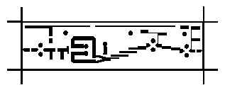
On the other hand the bandpass filter removes noise and undesired spectral components. Those undesired random contributions yield random fluctuations in amplitude and phase of the extracted clock signal. Of course, the phase noise contributes to timing jitter in the recovered data signal. A phase shifter is an important feature of all clock recovery circuits at high frequencies and should be contained in a clock recovery device. This phase shifter is necessary to equalize the different path lengths of the data and the extracted clock. One possible solution for generating a discrete spectral component is shown on the electrical circuit diagram. The circuit was developed as a part of an STM-64 (10 Gbps) NRZ clock recovery circuit. The circuit is built in microstrip on 0.8-mm-thick FR-4 laminate. The microstrip circuit board is shown in Figure 5.
Fig. 5 The microstrip circuit board.
Because the data signal in optical communications contains only positive and zero pulses, the capacitor at the input of the circuit removes the DC component of the signal. The signal is then amplified with the wideband amplifier. The signal is processed after the amplifier by the lowpass filter, making the square NRZ pulses round. The round pulses drive the full-wave rectifier, which comprises two diodes. Each diode generates a half-wave rectified signal. One of the half-wave rectified signals is delayed by a half-bit period and then combined with the other in the Wilkinson combiner. The signal is then filtered by two 10 GHz band pass filters to limit the power of unwanted spectral components to prevent saturation of the successive devices (for example, the mixers in the phase-locked loop (PLL)). The filters are built in microstrip as coupled resonators. Their quality factor (Q) is not high enough to extract the clock frequency out of the signal. Because the losses of the FR-4 laminate are quite large at 10 GHz, the circuit also contains two amplifiers composed of two ATF35376 high electron mobility transistors (HEMT). The measured signal before and after nonlinear processing is shown in Figure 6.
Although the full-wave rectifier was used to obtain the discrete clock frequency, any other even nonlinearity would accomplish the same result. Popular nonlinearities are a squarer or two-input XOR gate with one input delayed by half of the bit period.
The presence of discrete spectral lines in the spectrum of the RZ signal makes the clock recovery easier. The block diagram of a RZ clock recovery circuit is shown in Figure 7. Basically, the scheme is very similar to an NRZ clock recovery except for the absence of the nonlinear circuit, which is not necessary in this case.
BANDPASS FILTERING
The band pass filters used in a spectral line clock recovery circuit must have a Q above 1000. In general, two practically applicable types of filtering can be used. The straightforward configuration uses a dielectric resonator (DR).5,6 The attractive properties of the DR in such applications are high Q around 1000 and small dimensions. However, the disadvantages are relatively difficult precise mechanical manufacturing and static phase error due to the resonator's phase transfer function. This static phase error is a function of the frequency offset and, therefore, the deviations of the clock frequency cause deviations of the phase of the extracted clock. Finally, aging and temperature changes cause unknown random drifts of the resonant frequency, which again cause random phase errors of the recovered clock signal.
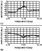
Fig. 6 The measured spectrum (a) before and (b) after the nonlinearity circuit
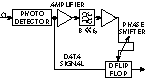
Fig. 7 A RZ clock recovery circuit.
It is important to note the problems related to scrambling. A scrambler is a device that modulo 2 adds a data signal and pseudorandom binary sequence, thus making the data signal more random. The scrambled signal therefore doesn't contain very long intervals of identical bits, which prevents the clock recovery circuit from losing the clock signal. The longer intervals of identical bits are allowed in the data signal the more difficult it is to recover the clock signal out of the scrambled signal. Since it is difficult to manufacture scramblers at the final bit rate (several gigabits per second) scramblers are used at lower bit rates of 155 or 622 Mbps. Therefore, the efficiency of scrambling at the final bit rate is smaller and requirements for clock recovery become more rigorous. Consequently, the Q of the clock recovery circuit's bandpass filter must be much greater than 1000, which is difficult to obtain even with a DR.
An alternative to the DR is a PLL. The PLL has certain advantages in comparison to high Q resonators. The PLL Q is inversely proportional to the bandwidth of the lowpass loop filter, which can be made arbitrarily small. The PLL does not have a static phase error, and this phenomena is frequency independent. The PLL component tolerances are uncritical and, therefore, the PLL is not difficult to fabricate. For the same reason, the PLL can be integrated in monolithic ICs. The major drawback of the PLL is the difficulty it has locking under the circumstances of the clock recovery operation. International Telecommunication Union specifications require very narrow bandwidth of the bandpass filter, which filters out the clock component. In the case of the PLL this means that the loop bandwidth of the PLL is much smaller than the frequency uncertainty of the VCO due to aging and temperature and supply voltage changes. Therefore, a simple PLL with one phase detector, a lowpass filter and a VCO never attains lock since the input signal is outside of the PLL capture range. To lock the PLL under such stringent conditions a more complicated PLL is required with an additional circuit that helps the PLL to lock on the input signal. An example of the PLL that can be used in the clock recovery is shown in Figure 8.2,3,4
Besides the usual circuitry the PLL also uses an integrator and an additional circuit to search lock. The integrator is used to prevent the clock recovery circuit from losing synchronization when long sequences of identical bits occur at the input of the clock recovery circuit. When this situation occurs, the previous voltage at the output of the phase detector is stored in the integrator and the VCO maintains the same frequency. Of course during normal operation, when the PLL is fed with a random data signal, a direct path to the VCO is also required. The direct path corrects noise and other short-term drifts in the VCO. This type of filter also got its name in regulation theory as the proportional plus integral filter (PI regulator in the example PLL circuit diagram).
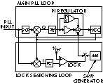
Fig. 8 An example of a PLL circuit used in clock recovery.
Another problem is the inability of the PLL to lock when the bandwidth of the loop filter is narrower than the frequency uncertainty of the VCO. One way to solve the problem is to use a quadrature phase detector.2,3 The quadrature Q output of the detector provides the feedback signal of the PLL. In the PLL's search mode a slow (10 Hz) sawtooth voltage is added to the Q output of the detector. This sawtooth voltage sweeps the VCO across the entire frequency range of the PLL. The in-phase I output of the VCO provides the lock information. When the PLL circuit locks, the I output stops the saw generator and the Q output takes control of the VCO. If the input signal is lost, the I output detects the loss of lock and begins sweeping the VCO again.
The PLL must be properly designed so as not to become unstable. The stability of the PLL is well covered in the literature1 so it will not be discussed here. It is important to note that the phase detector in the PLL causes one pole in the transfer function of the PLL and loop filter contributes additional poles. Besides stability, the PLL response should fulfill the jitter-tolerance and jitter transfer requirements.
CONCLUSION
At gigabit-per-second data rates, the most common technique for clock extraction is the spectral line method. Basically, the technique filters out a discrete spectral component at the clock frequency from the data signal spectrum. If a spectral line at the clock rate does not exist then a nonlinear circuit is required to process the signal to obtain this spectral line. First, the different data formats used in optical-fiber communications were presented. Then, the operation of the nonlinear circuit was described. Finally, two different techniques of clock-line filtering were presented.
ACKNOWLEDGMENT
The described model STM-64 clock recovery circuit was developed for use in field experiments as part of the European Community Esther ACTS 063 research project. The clock recovery circuit was tested at Pirelli Cavi e Sistemi SpA, Milano, which allowed the author to use its measuring equipment. The BAT 14-099 rectifier was manufactured by Siemens Semiconductors (now Infineon Technologies). The ATF-35376 HEMTs were manufactured by Avantek (now Agilent). The ERA-1 amplifier was manufactured by Mini-Circuits. The data plots in this article were obtained with an HP 8593 EM spectrum analyzer.
References
1. J. Smith, Modern Communication Circuits, McGraw Hill, 1986.
2. M. Vidmar, "K-band Quadrature Mixers with Plastic-packaged Diodes," Microwave Journal, Vol. 43, No. 1, January 2000, pp. 22-40.
3. M. Vidmar, "Microstrip Resonant Phase Shifters," Microwave Journal, Vol. 42, No. 9, September 1999, pp. 127-136.
4. S. Khursheed Enam et al. "NMOS ICs for Clock and Data Regeneration in Gigabit-per-second Optical Fiber Receivers," IEEE Journal of Solid-state Circuits, Vol. 27, No. 12, 1992, pp. 1763-1774.
5. Jae Ho Song et al. "10 Gbit/s Clock Recovery Circuit Using Temperature Compensated Dielectric Resonator Filter," Electronics Letters, Vol. 31, No. 17, August 1995, pp. 1458-1460.
6. P. Monteiro et al., "20 Gbit/s DR Based Timing Recovery Circuit," Electronics Letters, Vol. 30, No. 10, May 1994, pp. 799-800.
7. "80 Gbit/s Optical Clock Recovery Using an Electrical Phase Locked Loop and Commercially Available Components," OFC 2000, ThP4-1, March 2000, pp. 229-231.
8. L. Kazovsky et al., Optical Fiber Communication Systems, Artech House, 1996, pp. 471-512.