
EFFECTIVE CIRCUIT DESIGN TECHNIQUES TO INCREASE MOSFET POWER AMPLIFIER EFFICIENCY
Newly developed low cost and highly linear, high gain and high power laterally diffused metal oxide semi-conductor (LDMOS) and vertically diffused metal oxide semiconductor (VDMOS) field-effect transistors are attractive devices for many applications including commercial FM broadcasting and TV power transmitters, cellular and paging communication systems, and military RF and microwave hand-held transceivers. In all cases, along with high quality transmission of radio signals resulting from the high linearity of the amplifier transfer characteristic, it is necessary to provide high reliability and low overall dimensions of the power amplifiers along with an increase in total operating efficiency.
Fig. 1 Ideal class F voltage and current waveforms.
![]()
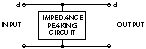
To obtain high efficiency of the power amplifier, it is advisable to use a tuned class B or Class F operating mode.1,2 In such amplifiers, the fundamental and harmonic load impedances are optimized by short-circuit terminations and open-circuit peaking in order to control the voltage and current waveforms at the drain of the device to obtain maximum efficiency.
CLASS F OPERATION
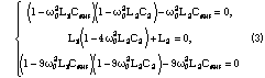
The impedance conditions at the drain of the device for 100 percent idealized drain efficiency must be1
![]()
where
Eds = drain supply voltage
Is = peak drain current
n = harmonic component
These impedance conditions correspond to the class F operating condition, the ideal voltage and current shapes for which are shown in Figure 1. Here a sum of odd harmonics produces a square voltage waveform and a sum of even harmonics approximates a half-sinusoidal current shape. In reality, both extrinsic and intrinsic transistor parasitic elements have a substantial effect on the efficiency, especially at high frequencies. By using only the active device die it is possible to reduce the influence of the parasitic elements in the power amplifier module. However, in this case it is necessary to take into account the main influence of the device output capacitance Cout .
The ideal class F amplifier with a voltage second-harmonic short-circuit termination and current third-harmonic peaking allows realization of the maximum drain efficiency of 75 percent.3 For a lumped-circuit amplifier, in order to approximate ideal class F operation with the harmonic impedance conditions of Z1 = Z3 = ∞ Ω and Z2 = ∞ Ω at the drain by compensating for the influence of Cout it is advisable to use an additional parallel circuit. An equivalent output impedance peaking circuit for a lumped-circuit amplifier is shown in Figure 2. The reactive part of the output admittance of this circuit is given by


Fig. 2 An output impedance peaking circuit.
Fig. 3 The two-port passive circuit's schematic for simulation.
Applying the previously mentioned three harmonic impedance conditions, open-circuited for the fundamental and third harmonic and short-circuited for the second harmonic, equation (2) can be rewritten in the form
where
w0 = 2p f0
f0 = fundamental frequency
As a result, the elements of the output impedance peaking circuit are

Fig. 4 The lumped impedance peaking circuit's frequency response.

Fig. 5 The microstrip amplifier's output impedance peaking circuit.
Linear analysis, which is sufficient to compute the response of a two-port passive circuit with lumped or distributed parameters, has been accomplished using the Serenade 7.5 CAD simulator. Simulations were performed according to the schematic shown in Figure 3 regarding the drain of the device. The frequency-response characteristic of a lumped impedance-peaking circuit (L1 = 7.7 nH, L2 = 12.8 nH, C2 = 5.3 pF) with a quality factor Q of 20 for the inductances at the fundamental frequency f = 0.5 GHz, and a device output resistance Rout of 200 Ω and output capacitance Cout of 2.2 pF is shown in Figure 4. To increase the total efficiency of the amplifier, the element of the output matching circuit adjacent to the drain of the transistor must be series and inductive in order to provide a high impedance for odd harmonic components.1
To increase maximum drain efficiency up to 88.4 percent, it is necessary to provide a short-circuit termination for all even-harmonic voltages and an open-circuit impedance for third-harmonic currents.3 Class F operation mode is easy to realize by using transmission lines in the output circuit. For a microstrip amplifier, it is enough to provide transmission lines with electrical lengths at the fundamental frequency of

where
Z0 = characteristic impedance of the microstrip line

Fig. 6 The microstrip impedance forming circuit's frequency response.
The equivalent output impedance peaking circuit of microstrip amplifier is shown in Figure 5. The frequency-response characteristic of the microstrip impedance-forming circuit on a substrate with dielectric loss tangent tan δ = 0.0001 featuring a device output resistance Rout of 50 Ω and an output capacitance Cout of 2.2 pF, with a characteristic impedance of the microstrip lines Z0 of 50 Ω and electrical length θ2 of 15 Ω is shown in Figure 6. It follows from the data that if the short-circuited conditions for all even voltage harmonics and current third-harmonic peaking are in place, then additional output matching is required at the fundamental frequency f0 = 0.5 GHz taking into account the reactance introduced by the impedance peaking circuit.
AMPLIFIER NONLINEAR CAD SIMULATION
The small-signal equivalent circuit of a high-power LDMOS FET cell with channel length L = 1.25 μm and channel width W = 1.44 μm is shown in Figure 7. The device model parameters were extracted from pulsed I-V and S-parameter measurements. The parameters of the equivalent circuit are given at a bias voltage for class AB operation with quiescent current Iq = 15 mA at Eds = 28 V.
Fig. 7 The LDMOS FET's small-signal equivalent circuit.

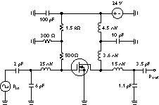
Fig. 8 The simulated 500 MHz one-stage lumped power amplifier's equivalent circuit.
The equivalent circuit of the simulated 500 MHz one-stage lumped power amplifier is shown in Figure 8. The total channel width of the high-voltage LDMOS FET is 7 × 1.44 mm. The drain efficiency and gain of the amplifier versus input power Pin for the case of ideal circuit inductances are shown in Figure 9. The obtained value of the drain efficiency of more than 80 percent is the result of additional harmonic peaking on higher components which allows a shortened switching time from the pinch-off region to the saturation region by better approximation of the drain voltage square waveform, as shown in Figure 10. However, the amplifier drain efficiency as well as the gain can reduce significantly in the case of sufficiently small values of a circuit inductance Q. For example, the maximum drain efficiency is only 71 percent when an inductance Q of 30 at the fundamental frequency is used, as shown in Figure 11.
Fig. 9 Drain efficiency and gain vs. input power.
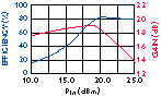

Fig. 10 The drain voltage waveform approximation.
Fig. 11 Drain efficiency and gain vs. input power when the inductances have a Q of 30.
![]()
Therefore, for high output power level, it is preferable to use matching circuits based on microstrip lines. In a simulated 500 MHz one-stage microstrip power amplifier, the input and output matching circuits are T-section matching circuits, and each of them consists of a series microstrip line, parallel open-circuit stub and series capacitance. To provide even harmonic termination and third-harmonic peaking for class F operation, an RF short-circuited quarter-wave microstrip line and combination of series microstrip line and open-circuit stub of λ/12 electrical length for third harmonic termination are used. Such an output circuit configuration closely matches the square drain voltage waveform, as shown in Figure 12 and a high value of drain efficiency up to 80 percent with maximum output power Pout = 9 Ω is obtained, as shown in Figure 13. The power amplifier's equivalent circuit is shown in Figure 14.

Fig. 12 The microstrip amplifier's drain voltage waveform.
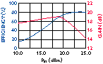
Fig. 13 The microstrip amplifier's drain efficiency and gain vs. input power.
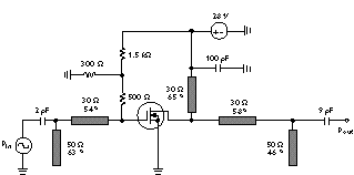
Fig. 14 The simulated 500 MHz one-stage microstrip power amplifier's schematic.
Fig. 15 The equivalent circuit of the simulated 500 MHz one-stage microstrip high-power amplifier using an LDMOS FET with a channel width of 28 × 1.44 mm.
However, a further increase of the total LDMOS FET channel width leads to an increase of Cout and, as a result, to a decrease in electrical length of the series microstrip line adjacent to the drain, the value of which becomes too small to provide appropriate third harmonic peaking. In this case, in order to realize both high efficiency and high power operation, the output circuit must be simplified to only a T-section for impedance matching. The equivalent circuit of the simulated 500 MHz one-stage microstrip high-power amplifier with a total LDMOS FET channel width W = 28 × 1.44 mm is shown in Figure 15. As it turned out, a significant improvement of drain efficiency up to 78 percent for an output power of approximately 30 W can be realized by using the specific electrical length (less than quarter-wave length) of parallel microstrip line, as shown in Figure 16. Furthermore, the analysis of the drain voltage and current waveforms, shown in Figure 17, demonstrates that the operating mode obtained is close to class E operation mode.5 As seen in the data, when the transistor is turned on, there is practically no voltage when the drain current achieves its maximum value. On the other hand, when the transistor is turned off, the drain current continues to flow, but now only through the shunt output capacitance Cout . The appropriate required reactive harmonic load impedance of the external circuit is realized by the open-circuit stub at the second harmonic whose electrical length is approximately 0.125λ and by the RF short-circuit microstrip line whose impedance is sufficiently small at the third harmonic. At the same time this output circuit configuration accomplishes effective fundamental impedance matching of the output transistor impedance with the load.
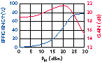
Fig. 16 Drain efficiency and gain vs. input power for the T-section impedance.
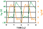
Fig. 17 Drain voltage and current waveforms using the T-section impedance matching configuration.
EXPERIMENTAL RESULTS
The experimental test structure of a single-stage LDMOS FET power amplifier with a device gate length of L = 1.25 μm and total gate width of W = 4 cm is shown in Figure 18. Two T-section transformers with series microstrip lines and parallel variable capacitors have been used as the input and output matching circuits. The matching circuits were fabricated on epoxy glass copper-clad laminate substrates and the characteristic impedance of all microstrip lines is equal to 50 Ω. To avoid low-frequency parasitic oscillations, a 10 μF electrolytic capacitor was connected in parallel with the drain supply. The parameters of the matching circuit elements and the length of the microstrip line in the drain supply circuit were chosen according to the results of the CAD simulation for a high-efficiency operating mode of the power amplifier. Only small fine tuning of the variable capacitors in the input and output matching circuits was required to realize excellent electrical characteristics of the given LDMOS FET power amplifier.
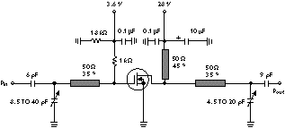
Fig. 18 The single-stage LDMOS FET power amplifier's experimental test structure.

Fig. 19 Measured drain efficiency and gain vs. power input.
The drain efficiency and power gain characteristics as a function of input power are shown in Figure 19. An output power of 20 W max with a drain efficiency of 76 percent and DC collector current of 0.94 A has been achieved. A practically constant small-signal power gain of approximately 17 dB was achieved over a wide dynamic range up to an input power of 25 dBm as a result of the appropriate choice of gate bias voltage.
ACKNOWLEDGEMENT
The author would like to thank Fujiang Lin for on-wafer measurements and device modeling as well as for helpful discussions and support. The Serenade 7.5 simulator is a product of Ansoft Corp., Pittsburgh, PA.
References
1. D.M. Snider, "A Theoretical Analysis and Experimental Confirmation of the Optimally Loaded and Overdriven RF Power Amplifier," IEEE Trans. Electron Devices, Vol. 14, December 1967, pp. 851-857.
2. H.L. Krauss, C.W. Bostian and F.H. Raab, Solid State Radio Engineering, New York: Wiley, 1980.
3. F.H. Raab, "Class-F Power Amplifiers with Maximally Flat Waveforms," IEEE Transactions on Microwave Theory and Techniques, Vol. 45, November 1997, pp. 2007-2012.
4. C. Duvanaud, S. Dietsche, G. Pataut and J. Obregon, "High-efficient Class F GaAs FET Amplifiers Operating with Very Low Bias Voltages for Use in Mobile Telephones at 1.75 GHz," IEEE Microwave and Guided Wave Letters, Vol. 3, August 1993, pp. 268-270.
5. T.B. Mader, E.W. Bryerton, M. Markovic, M. Forman and Z. Popovic, "Switched-mode High-efficiency Microwave Power Amplifiers in a Free-space Power-combiner Array," IEEE Transactions on Microwave Theory and Techniques, Vol. 46, October 1998, pp. 1391-1398.