
Responding to ever-increasing demands for higher data rates, wireless infrastructure providers are moving to more broadband systems. The newly-released 600 MHz spectrum (band 71) will help address these bandwidth needs. To take advantage of this spectrum, cellular base station operators need to provision amplifiers that operate from 600 MHz to 1 GHz. A wideband driver that covers all the individual bands, plus broadband applications below 1 GHz, with flat RF performance is desired for base station amplifier lineups, to achieve faster cycle time, ease of use and compact designs. To meet this market requirement, Infineon Technologies has developed a two-stage, 50 V, LDMOS RF integrated circuit (PTGA090304MD) that operates from 575 to 960 MHz.
LDMOS technology has long been the most cost-effective solution for base station power amplifiers (PA). Even though GaN has made significant progress in recent years, LDMOS is still the leading technology for commercial base station PAs below 1 GHz, due to its competitive RF performance and cost advantage. Unlike the traditional LDMOS process that uses a 28 V drain supply, Infineon’s 50 V LDMOS technology is optimized for 50 V, offering higher power density and competitive RF performance to meet market needs for more compact base station PAs.
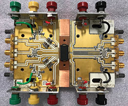
Figure 1 LDMOS driver IC in the broadband fixture.
DESIGN AND PERFORMANCE
The PTGA090304MD is a two-stage design based on Infineon’s 50 V LDMOS technology that operates from 575 to 960 MHz. By integrating two gain stages onto one IC, assembled in the low-cost TO270-14 over-molded plastic package, the device produces more than 30 dB gain and eliminates the need to use three discrete driver devices to meet the gain requirement of the lineup. The input is internally matched to 50 Ω, so no input matching is needed on the PCB. The DC blocking capacitor at the input is also integrated on the IC die.
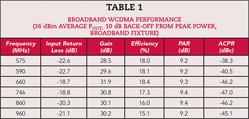
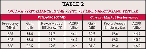
The PTGA090304MD covers 575 to 960 MHz, which corresponds to 50 percent fractional RF bandwidth, with one broadband impedance match on the PCB. Figure 1 shows the broadband RF fixture, and Table 1 summarizes the performance in the fixture with a single-carrier, 10 dB peak-to-average ratio (PAR), WCDMA waveform at 10 dB back-off from the peak power of 40 W. The device has flat output power, greater than 15 percent efficiency and 30 dB gain. The PTGA090304MD delivers competitive narrowband performance in the two major cellular bands under 1 GHz. Tables 2 and 3 show the RF performance at 10 dB output power back-off in the 728 to 768 and 920 to 960 MHz bands, respectively. The driver has 33 dB gain, 19 percent efficiency and excellent raw linearity of -46 dBc adjacent channel power ratio (ACPR) in both bands.
The PTGA090304MD’s output match uses a simple matching topology that is easy to implement on the PCB, making impedance tuning straightforward and convenient to implement in production. The same PCB layout (see Figure 1) is used for the broadband and two narrowband fixtures, as the output match for the different frequency bands only requires changing two surface-mount capacitors. This provides the flexibility of using one device and one board layout to cover multiple bands, minimizing manufacturing complexity.
Being a dual-path device, the PTGA090304MD can be used in different amplifier architectures. The circuit in Figure 1 shows the device operating in class AB, with both paths split and combined with a 3 dB hybrid coupler on the input and output, respectively. To achieve higher efficiency, the two devices can be configured as carrier and peaking amplifiers in a broadband Doherty configuration.
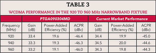
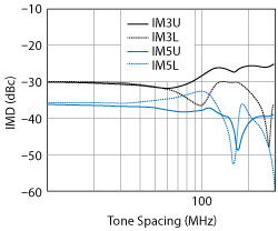
Figure 2 Two-tone IMD vs. tone spacing, with the driver in the broadband fixture.
Excellent raw linearity at the device level helps to reduce the complexity and cost of external linearization or to increase the output power and efficiency. Figure 2 shows the two-tone IMD performance versus tone spacing. Linearization of the device was characterized using an Optichron digital predistortion (DPD) system. With DPD, the ACPR of the circuit was reduced to the noise floor of -54 dBc, using a two carrier LTE signal with 7.9 dB PAR and 40 MHz signal bandwidth, showing no RF performance degradation at 7 dB back-off from the peak power.
The PTGA090304MD wideband IC provides state-of-the-art performance below 1 GHz and meets the requirements of base station PAs. Scheduled for production in the third quarter of 2018, it will have the widest bandwidth of any 1 GHz RFIC on the market—while offering competitive narrowband performance. Infineon plans future two-stage ICs using 50 V LDMOS, for different power levels.
Infineon RF
Morgan Hill, Calif.
www.infineon.com/rfpower