
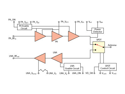
Although 5G systems will require linear amplification to preserve modulation fidelity, the output referred P1dB and PAE were also measured to provide a figure of merit for comparative purposes. The measured performance is shown in Figure 8 and shows a P1dB around 20.2 dBm, which rises to 21 dBm at saturation. The PAE of the FEM Tx path is around 20 percent, falling slightly at the top of the band.
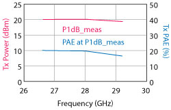
Figure 8 Measured P1dB and PAE of the Tx path vs. frequency.
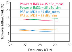
Figure 9 Measured and simulated Tx power and PAE operating at ~7 dB backed-off.
As mentioned above, the FEM is designed for optimum performance (OIP3 and PAE) when operated at around 7 dB backed-off from P1dB, specifically with the IMD3 at a level of below ‐35 dBc relative to the wanted products during a two-tone test with 100 MHz tone spacing. This operating point is close to that envisaged in the 5G system for which the FEM was designed.
Figure 9 shows a plot of the measured and simulated PAE and total RF output power when operating at an IMD3 point of ‐35 dBc. The measured PAE is 6.5 percent, which is good and largely due to the PA being designed to operate in deep class AB. The total RF output power is around 13.5 dBm, which equates to an OIP3 level of +28 dBm.
The on-chip Tx power detector characteristic provides a DC voltage that allows monitoring of the RF output power. The temperature compensated detector output “Vref-Vdet” is plotted in mV on a logarithmic scale against output power in dBm over a 15 dB dynamic range in Figure 10. On this scale the characteristic is linear making power monitoring easier.
Figure 10 FEM Tx on-chip power detector measured characteristics at 28 GHz.
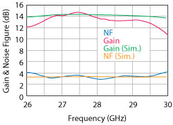
Figure 11 Rx path measured and simulated gain and NF.
When the Rx path of the FEM is selected the PA is powered down, “Vctrl1” is set to 0 V and the LNA biased to around 10 mA from +4 V with 3.9 V observed on the “LNA_Vsense” pin. Figure 11 is a plot comparing the measured and simulated gain and noise figure (NF). The measured small signal gain is around 13.5 dB with a gain flatness of just ±0.3 dB across the band. The Rx path has an excellent noise figure of typically 3.3 dB from 27 to 29 GHz with good agreement between simulated and measured performance.
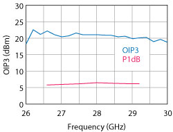
Figure 12 Rx path measured P1dB and OIP3.
The Rx path also demonstrates impressive linearity for the modest power consumption (just 40 mW: 10 mA at 4 V). Key parameters such as P1dB and OIP3 are around 6.2 and 21 dBm, respectively, across the band. Figure 12 is a plot of the measured P1dB and OIP3 versus frequency.
Conclusion
The FEM MMIC described here will potentially play a key role in future 28 GHz, 5G systems. The part has been shown to address all the requirements for integration into mmWave phased-array or beam switched terminals and offers excellent Tx linearity and efficiency together with outstanding Rx noise figure. The key performance specifications for both transmit and receive paths were met, ensuring that the part is highly suitable for mm-Wave 5G applications. The IC also includes useful features such as a Tx power detector, Tx and Rx enable circuits, an SPDT decoder circuit and Rx bias monitoring. Realized on a state of the art 0.15 µm enhancement mode GaAs PHEMT process the part is extremely easy to control and monitor using widely available multi-channel ADC and DAC ICs. In addition, the part is conveniently housed in a compact and low cost 5 mm × 5 mm plastic overmolded QFN SMT package.
References
- L. Devlin, “The Design of Integrated Switches and Phase Shifters,” Proceedings of the IEEE Tutorial Colloquium on Design of RFICs and MMICs, November 24, 1999, pp. 2/1-14.
- S. Glynn and L. Devlin, “The Design of a Dual-Band PA for mmWave 5G Applications,” Proceedings of the RF and Microwave Society (ARMMS) Conference, November 13, 2017.