

Cost Analysis
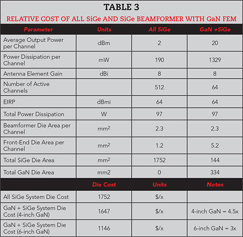
The cost of phased arrays include the RF components, printed circuit board material and the antennas themselves. Using compound semiconductor front-ends allows an immediate 8x reduction in array size with no increase in PDISS. Even with lower-cost printed antenna technology, this is a large saving in expensive antenna-quality substrate material. Considering component cost, the current die cost per mm2 of 150 nm GaN on SiC fabricated on 4-inch wafers is only 4.5x the cost of 8-inch 130 nm SiGe. As 6-inch GaN production lines shift into high volume, the cost of GaN relative to SiGe drops to 3x. A summary of the assumptions and a cost comparison of the relative raw die cost of the two technologies is shown in Table 3. Using a high-power density compound semiconductor like GaN on 6-inch wafers can save up to 35 percent in the raw die cost relative to an all-SiGe architecture. Even though the cost of silicon technologies is lower per device, the cost of the complete system is significantly higher.
GaN FRONT-END MODULES
To validate the concept of a GaN FEM for mmWave FWA arrays, Qorvo set out to design the highest power, lowest NF FEM for the 37 to 40 GHz band. To support the trend to integrated transmit/receive arrays, the front-end includes a PA, integrated T/R switch and a low NF LNA. The module was designed with sufficient gain to be driven by core beamformer RFICs, which have a typical drive level of 2 dBm. The FEM’s PAVE of 23 dBm was selected from an analysis similar to that shown in Figure 16, and the PSAT was determined by analyzing the needed headroom to support a back-off linearity of ≥ 33 dBc ACPR, EVM ≤ 4 percent and a 400 MHz orthogonal frequency-division multiple access (OFDMA) waveform.
A key design decision was determining if GaAs or GaN or a combination of both were needed. The die size for a GaAs PA would not allow the FEM to meet the tight 3.75 mm lattice spacing at 39 GHz. The equivalent output power GaN PA is 4x smaller with no sacrifice in gain and a slight benefit in efficiency. Considering the LNA, the 90 nm GaAs PHEMT process was favored due to its slightly superior NF. However, the net improvement was only a few tenths of a dB once the additional bond wires and 50 Ω matching networks were considered. The trade-off analysis concluded it was better to stay with a monolithic GaN design that allowed co-matching of the PA, LNA and T/R switch. Such a design was lower risk, easier to assemble and test, and the MMIC was as compact as possible. The system thermal analysis indicated that the higher junction temperature offered by GaN-on-SiC was critical for passively-cooled arrays.
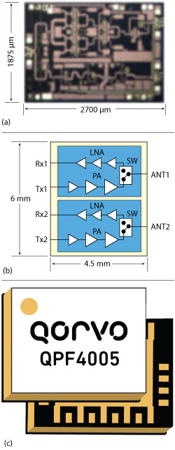
Figure 17 Integrated 39 GHz GaN front-end MMIC – intentionally blurred (a), dual-channel FEM (b) and package (c).
As shown in Figure 17, the 39 GHz FEM integrates two of the multi-function GaN MMICs into an air-cavity, embedded heat-slug, surface-mount package, sized to meet the array element spacing at 39 GHz. Each of the GaN MMICs contains a three-stage linear PA, three-stage LNA and a low-loss, high-linearity SPDT switch. The FEM covers 37.1 to 40.5 GHz and provides 23 dBm average output power, which supports 256-QAM EVM levels, with 24 dB transmit gain. In receive mode, the NF is 4.1 dB, and receive gain is 16 dB. The package size is 4.5 mm × 6.0 mm × 1.8 mm.7-8
SUMMARY
FWA is rapidly approaching commercialization. This is due to the abundance of low-cost spectrum, early regulatory and standards work and the opportunity for operators to quickly tap a new market. The remaining challenge is the availability of equipment capable of closing the link at a reasonable cost. Both hybrid beamforming and all-digital beamforming architectures are being explored. These architectures capitalize on the respective strengths of commercial semiconductor processes. The use of GaN front-ends in either approach provides operators and manufacturers a pathway to achieving high EIRP targets while minimizing cost, complexity, size and power dissipation. To prove the feasibility, Qorvo has developed a 39 GHz FEM based on a highly integrated GaN-on-SiC T/R MMIC and is developing similar FEMs for other millimeter wave frequency bands proposed for 5G systems.
References
- International Telecommunications Union, ITU-R Radiocommunications Sector of ITU, “IMT Vision–Framework and Overall Objectives of the Future Development of IMT for 2020 and Beyond,” August 2015, www.itu.int/dms_pubrec/itu-r/rec/m/R-REC-M.2083-0-201509-I!!PDF-E.pdf.
- International Telecommunications Union, Resolution 238 (WRC-15), “Studies on Frequency-Related Matters for International Mobile Telecommunications Identification Including Possible Additional Allocations to the Mobile Services on a Primary Basis in Portion(s) of the Frequency Range 24.25 and 86 GHz for Future Development of IMT-2020 and Beyond,” 2015, www.itu.int/dms_pub/itu-r/oth/0c/0a/R0C0A00000C0014PDFE.pdf.
- Federal Communicationws Commission, “Use of Spectrum Bands Above 24 GHz for Mobile Radio Services, In the Matter of GN Docket No. 14-177, IB Docket No. 15-256, RM-11664, WT Docket No. 10-112, IB Docket No. 97-95,” July 2016, apps.fcc.gov/edocs_public/attachmatch/FCC-16-89A1.pdf.
- 3GPP TR 38.901, “Study on Channel Model for Frequencies from 0.5 to 100 GHz,” September 2017, www.3gpp.org/ftp//Specs/archive/38_series/38.901/38901-e20.zip.
- A. F. Molisch et al., “Hybrid Beamforming for Massive MIMO: A Survey,” IEEE Communications Magazine, Vol. 55, No. 9, 2017, pp. 134–141.
- B. Sadhu et al., “7.2 A 28GHz 32-Element Phased-Array Transceiver IC with Concurrent Dual Polarized Beams and 1.4 Degree Beam-steering Resolution for 5G Communication,” 2017 IEEE International Solid-State Circuits Conference (ISSCC), San Francisco, Calif, 2017, pp. 128–129.
- B. Kim and V. Z. Q. Li, “39 GHz GaN Front-End MMIC for 5G Applications,” 2017 IEEE Compound Semiconductor Integrated Circuit Symposium (CSICS), Miami, Fla., 2017, pp. 1–4.
- “QPF4005 37-40.5 GaN Dual Channel FEM Datasheet,” www.qorvo.com/products/d/da006271.