
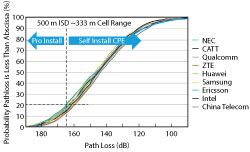
Figure 5 Statistical path loss simulation for urban-macro environment with 500 m ISD.
FWA Link Budget
The standards community has been busy defining the performance requirements and evaluating use cases over a broad range of mmWave frequencies. The urban-macro scenario is the best representation of a typical FWA deployment: having large ISD of 300 to 500 m and providing large path-loss budgets that overcome many of the propagation challenges at mmWave frequencies. To understand the needed link budget, consider a statistical path-loss simulation using detailed large-scale channel models that account for non-line-of-site conditions and outdoor-to-indoor penetration, like those defined by 3GPP.4 Figure 5 shows the result for a 500 m ISD urban-macro environment performed by equipment vendors and operators. For this simulation, 28 GHz channel models were used with 80 percent of the randomly dropped users falling indoors and 20 percent outdoors. Of the indoor users, 50 percent were subject to high penetration-loss models and 50 percent lower loss. Long-term, carriers desire at least 80 percent of their potential users to be self-installable to minimize more expensive professional roof-level installations. The distribution curve shows the maximum system path loss to be 165 dB.
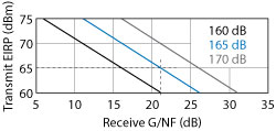
Figure 6 Transmit EIRP and receive G/NF vs. path-loss for 1 Gbps edge-of-coverage throughput.
Closing the link depends on many variables, including transmit EIRP, receive antenna gain, receiver noise figure (NF) and minimum edge-of-coverage throughput. To avoid overdesign of the cost-sensitive CPE equipment and shift the burden toward the BTS, the link design begins at the CPE receiver and works backward to arrive at the BTS transmitter requirements. In lieu of the conventional G/T (the ratio of antenna gain to system noise temperature) figure-of-merit (FOM), we define a more convenient G/NF FOM: the peak antenna gain (including beamforming gain) normalized by the NF of the receiver. Figure 6 illustrates the required EIRP for the range of receive G/NF to overcome a targeted path loss delivering an edge-of-coverage throughput of 1 Gbps, assuming the modulation spectral efficiency is effectively 2 bps/Hz and demodulation SNR is 8 dB. From the graph, the BTS EIRP for a range of CPE receiver’s G/NF can be determined. For example, 65 dBm BTS EIRP will be needed to sustain a 1 Gbps link at 165 dB of path loss when the CPE receiver G/NF is ≥ 21 dBi.
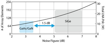
Figure 7 Array size vs. front-end NF and power consumption for G/NF = 21 dB.
Next, we consider the impact of receiver NF by plotting the minimum number of array elements needed to achieve G/NF of 21 dB (see Figure 7). We also plot the total low noise amplifier (LNA) power consumption. By adjusting the axis range, we can overlap the two and see the impact NF has on array size, complexity and power. For this example, each LNA consumes 40 mW, which is typical for phased arrays. The NFs of RFFEs, including the T/R switch losses, are shown for 130 nm SiGe BiCMOS, 90 nm GaAs PHEMT and 150 nm GaN HEMT at 30 GHz. The compound semiconductor technology provides ≥ 1.5 dB advantage, translating to a 30 percent savings in array size, power and, ultimately, CPE cost.
To explore architecture trades that are key to technology selection and design of the RFFE components, we start by understanding the antenna scanning requirements. We highlight the circuit density and packaging impact for integrated, dual-polarization receive/transmit arrays. Finally, we investigate all-digital beamforming and hybrid RF beamforming architectures and the requirements for each.