

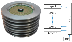
Figure 11 Plasma Antenna 360° field of view beamforming and steering 28 GHz, 5 W, 16 dBi gain PSiAn.
PSiAn uses either single or multiple PSiDs to perform azimuth and elevation beam steering. The PSiDs are mounted on RF PCBs and use transmission lines to link the device ports to traditional RF and antenna technologies, such as LNAs, PAs, printed feeds, lenses and reflectors to produce efficient smart antennas with steerable narrow beams. Potential applications of PSiAn plasma antennas include: small cell backhaul at V-Band (60 GHz), gigabit wireless LAN (e.g. WiGig), intelligent transport systems (ITS) at 63 GHz and vehicle radar (77 GHz).
The company recently introduced an antenna that reduces the cost of a 5G base station by up to 50 percent by eliminating phase shifters, reducing and consolidating amplification and reducing computation. The technology does not need calibration and can handle high-power, having been tested up to 40 W. The company has shown the technology in a variety of scenarios, including a 360 degree field of view, beamforming and steering, 28 GHz, 5 W, 16 dBi gain PSiAN, useful for pole mounted small cells, indoor small cells—also on a vehicle and a high-power, long range, low loss small cell base station antenna for standalone and MIMO 5G, fixed wireless access (FWA) and connected vehicle applications (see Figure 11).9 These devices can also be stacked to form and steer beams in two dimensions (azimuth and elevation) or to form multiple beams and MIMO applications.
They also announced their mmWave PSiAn for use in smartphones and other consumer electronics, delivering high throughput with low latency and utilizing directional beams that generate less interference and maximize energy efficiency.10 The introduction of mmWave connectivity for smartphones and other mobile devices faces significant problems as the signals are easily blocked by fingers, hands, heads and bodies. When used in combination with distributed radiating elements, PSiDs can be used as a switch and beam former to utilize only elements that are able to receive and transmit line-of-sight or reflected signals resolving this issue. Plasma Antennas recently modeled plasma silicon corner antennas as replacements for array modules for device manufacturers and silicon suppliers. This approach closely represented the publicly available solutions from Qualcomm and Samsung, for which there are many handling scenarios that would block the antennas. The array Plasma Antennas proposes now solves these problems and brings the intrinsic qualities of plasma silicon.
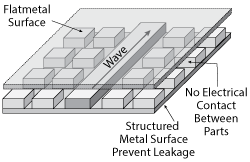
Figure 12 Gap waveguide structure.
Gapwaves AB was founded in 2011 by Professor Per-Simon Kildal at Chalmers University of Technology in Gothenburg, Sweden, with the aim of enabling efficient wireless communication through the patented GAP waveguide technology. GAP waveguides provide a unique packaging technology for mmWave and terahertz circuits and components, with advantages compared to existing transmission line and waveguide technology. The technology is based on an artificial magnetic conductor that enables contactless propagation of electromagnetic waves, significantly reducing transmission losses. The GAP waveguide is built up of two parts: a structured metal surface and a flat metal surface placed close to one another, allowing for an air gap between the two part (see Figure 12).11 The structured surface is characterized by pins forming a barrier, preventing the electromagnetic waves from propagating in undesired directions. In this way, the pins replace the walls in traditional rectangular waveguides without requiring perfect metallic contact. The waves are guided by ridges or grooves within the pin structure and propagate in air, resulting in low power losses. Antennas based on the GAP technology have more than 10x lower losses than micro strip lines, more than 3x lower losses than substrate integrated waveguide (SIW) and approximately the same losses as rectangular waveguides.11
As no metallic contact is required between the layers, the assembly of multilayered, closely spaced waveguide structures is simplified. The antenna layers can be glued together with no screws, pressure or heat. Production of the antenna parts is accomplished using plastic injection molding in combination with metallization or using die-casting in metal, resulting in high volume capabilities and a cost-efficient manufacturing process. The low power losses enable broadband antenna arrays with gains up to 38 dBi to be achieved with above 80 percent efficiency. The design flexibility that comes from using multilayered waveguide structures enables tailoring of the radiation pattern, as demonstrated by a recently developed 38 dBi E-Band antenna that has achieved ETSI class 3 radiation pattern performance.