

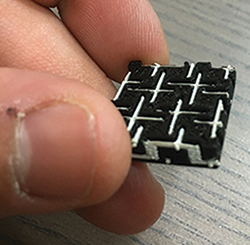
Figure 5 A small test coupon of MITRE’s biaxial metamaterial created with a Voxel8 multi-material 3D printer.
As covered in the October 2016 issue of Microwave Journal, The MITRE Corporation is investigating a new generation of 3D printing to realize the complex geometries of wideband phased array and metamaterial designs using commercial, low-cost, compact, desktop printers.1 Samples of the 3D printed plastic and conductive ink printed at room temperature were characterized over frequency. The polylactic acid (PLA) dielectric constant and loss tangent are found to be stable up to 18 GHz. The PLA internal architecture was varied to achieve lower effective dissipation factors, which extends usefulness to high frequency applications. Microstrip line samples were fabricated with simulated and measured insertion loss data validating the high conductivity through mmWave frequencies. A 3D printed monopole Wi-Fi antenna was built and tested, showing good performance and agreement with simulations.
MITRE also has developed a wideband phased array concept that has a complex metamaterial design. It is based on a PCB design that was not physically realizable with traditional manufacturing. The design resembles an egg-crate construction with contiguous electrical connection (interdigitiated fingers) that is embedded within the orthogonal board interface, as illustrated in Figure 5.1 Multi-material additive manufacturing is thought to be the only practical way to realize this design. They successfully printed a sample of the cross in the middle of the array, and a CT-scan showed the details of all of the fingers confirming the construction and working on full scale antenna structures.
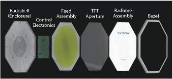
Figure 6 Kymeta mTenna™ construction.
Metamaterial Based Antennas
Metamaterials are made by arranging naturally occurring materials in a specific pattern that produces an electromagnetic response that is not found in nature. The periodic structures created are at scales that are smaller than the wavelengths of the phenomena they influence and can create materials with negative indexes that control electromagnetic energy in ways that cannot be done with natural materials. In traditional active electronically scanned arrays (AESA), phase shifters embedded in control circuitry steer the beam direction. Metamaterial-based AESAs can steer the beam without phase shifters, which reduces system complexity, eliminates a source of power loss and simplifies waste-heat dissipation. There are a couple of companies using unique metamaterial structures developed for this application.
Kymeta experimented with these structures for many years and discovered that the metamaterials could be used to form holographic beams that could link to satellites and maintain the link while the antenna is in motion. Kymeta mTenna™ technology (see Figure 6) is manufactured using a completely different process and components than both traditional antennas and phased array antennas.2 The “metamaterial” in mTenna technology is a metasurface in a glass structure. Their glass-on-glass structure is manufactured on the same production lines as LCD flat screen televisions, making it suited for low-cost, high volume manufacturing. They use the thin film transistor liquid crystal as a tunable dielectric. Instead of reflecting microwaves like a traditional dish antenna or creating thousands of separate signals like a phased array, Kymeta uses a thin structure with tunable metamaterial elements to create a holographic beam that can transmit and receive satellite signals.
They use software to steer the antenna, eliminating the need for mechanical gimbals to point the antenna toward a satellite. The antenna does not require active phase shifters or amplifiers. Key features of the approach:3
- Transmit and receive via a single aperture
- Wide angle scanning and excellent beam performance
- Electronically controlled pointing and polarization
- Extremely low power consumption
- First electronically scanned antenna designed for mass production.