
Abstract
 RF sampling technology, already available in L-, S- and C-Bands, allows acquiring the whole operative RADAR bandwidth. In this context, to overcome digital processing bottlenecks, an innovative FPGA based algorithm, targeting wide band RADAR signal has been designed. The algorithm is able to digitally process wide band signals, with a FPGA operative clock frequency much lower than the one requested by standard Nyquist-based processing. The same algorithm can also be used to reduce the FPGA operating clock frequency and therefore power consumption, a burning issue for small form factor modules. The algorithm is characterized in terms of functionalities, performance and FPGA implementation; an actual case study is presented.
I. Introduction
 Common defense RADAR systems implement frequency hopping technique as a countermeasure against enemy threats: a narrow band signal is generated inside the RADAR operative bandwidth and then frequency-shifted by the Agile Local Oscillator (ALO). Signals characterized by wide instantaneous bandwidth are instead required for imaging, communication and high-resolution applications. State of the art Radio Frequency (RF) sampling allows sampling the whole RADAR operative bandwidth1,2 at sub-array or even at radiating element level. With this new approach, standard analog functionalities, such as frequency agility, can now be realized in digital domain. Although modern technology offers Analog Digital Converter (ADC) devices with high sample rate, current Field Programmable Gate Array (FPGA) devices do not reach clock frequency able to manage such signals, being at a first glance the real limitation to this new approach in RADAR architecture. To overcome this limitation and realize a wide band fully digital receiver module, a new signal processing technique is presented, which makes it feasible the management of wide band signals on standard commercial FPGAs.
II. Wide Band Fully Digital Receiver: Architecture and Drawbacks
 Latest generation of ADCs (e.g. the ADC12DJ3200 by Texas Instruments and the AD9208 by Analog Devices) features RF analog band, clock frequency greater than 6 GSps and at least 12 bits vertical resolution; typically interface to/from FPGA is managed with standard high speed protocol like JESD204B. Such a device is a technological breakthrough in the design and realization of a compact fully digital receiver. In this kind of architectural solution, traditional front-end RADAR functionalities, such as frequency tuning, filtering and down conversion, migrate to the digital section.
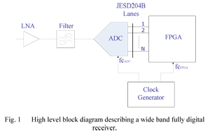
The scheme of principle of the wide band fully digital receiver is shown in Figure 1: the received signal is amplified, filtered and digitized directly around the carrier frequency. The analog and RF channels are greatly simplified since super-heterodyne architecture disappears and phase and amplitude correction as well as beam forming network can be digitally realized in FPGA. Size and weight reduction related to this solution will make it easier to set the receiver module at different hierarchical levels of the RADAR, from sub-array to radiating element. 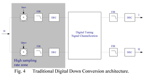
In such a context, one of the major challenges is to realize algorithms that can effectively realize in digital domain what is traditionally realized with analog hardware, being able to manage huge amount of data, no longer required only for wide band RADAR applications but now mandatory in the fully digital receiver architecture, since super-heterodyne is no longer existing.
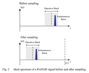
According to the Nyquist theorem3 the ADC sampling clock must be at least twice the acquired band, as shown in Figure 2. The grey box represents the operative band and the blue one is the instantaneous band, narrower than the operative one in traditional RADAR application.
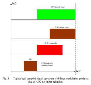
 To either avoid or to mitigate in-band ADC non linearity, the ADC sampling rate can reach values higher than twice the acquired band. A possible scenario is shown in Figure 3 where the acquired signal has a bandwidth of the order of hundreds MHz and it is sampled with a sampling frequency of the order of GHz. Furthermore, a high sampling clock reduces the noise spectral density (and increases the dynamic range) of the ADC.4
In RADAR conventional real time processing, for instance the Digital Down Conversion (DDC) algorithm shown in Figure 4, the FPGA working clock must be the same as the ADC sampling clock: since commercial FPGA devices typically do not exceed 500 MHz clock frequency, a conventional real time processing seems to be the real limitation for a wide band fully digital receiver. In this paper, an innovative DDC algorithm is proposed to overcome this limitation.
III. Innovative Digital Down-Conversion Algorithm for Wide Band Fully Digital Receiver: An Actual Case Study
 Figure 4 shows the traditional architecture for a DDC. By means of two Numerically Controlled Oscillator (NCO) blocks (Inco and Qnco) the whole RADAR operative bandwidth is shifted to base band, then a first signal decimation (FIR+DEC) is performed in order to reduce the following computational effort. In narrow band RADAR applications, the digital tuning is used to select the instantaneous band within the operative band, subsequently filtering and decimation are implemented to reject out-of-band signals as well as to reduce noise power.
 In Figure 4 the grey box shows the FPGA section that must work, in traditional real time processing, with the same clock as the ADC sampling clock, making this approach impossible for sampling rate of the order of GSps. The innovative algorithm presented in this paper is based on an alternative architecture for the grey box in Figure 4, able to process the signal with a FPGA clock rate lower than the ADC sampling rate.
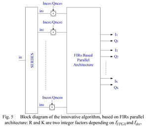
The starting point of the algorithm is the design of a traditional DDC in which original ADC sampling clock (fc), NCO frequency value, Finite Impulse Response (FIR) filter and base band signal decimation rate (fdec) are defined. Then, once decided FPGA working frequency (fFPGA), a parallel implementation of both NCOs and filtering is realized. A top level block diagram of the proposed architecture is shown in Figure 5. 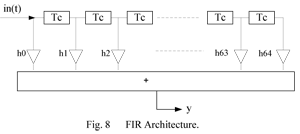
As case study for the described parallel DDC algorithm, an ADC sampling clock of 5 GHz with 12 bits vertical resolution and a signal bandwidth of 500 MHz with carrier in the C-Band are considered: this is an actual scenario for the wide band fully digital receiver shown in Figure 1.
 In this example, the parallel architecture is implemented with a FPGA clock frequency fFPGA equal to 312.5 MHz and a signal decimation rate fdec equal to 1.25 GHz. The SERDES block of Figure 5 divides the samples of the input signal, coming from the ADC at 5 GSps, into 16 flows at 312.5 MSps. For the NCOs, a frequency value of 625 MHz is chosen. Frequency scenario for the case study is shown in Figure 6.
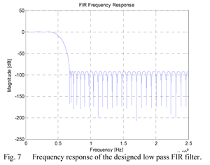
An important topic concerning the algorithm is the design of the native low pass FIR. It must select the operative band [-125 ÷ 375] MHz and remove image frequencies [-1625 ÷ -1125] MHz. Furthermore, the design of the FIR must be in accordance with the decimation performed at its output, selected to be 1.25 GSps. Figure 7 shows the frequency response of the designed FIR. 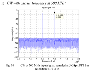
Pass band is at 380 MHz, stop band is at 675 MHz and out band rejection is equal to 95 dBc. Its order is 64. The filter presents the typical architecture of a FIR, shown in Figure 8.
Starting from the native FIR, it is possible to calculate all the FIRs used in the parallel architecture shown in Figure 5.
In our case study, the parallel architecture provides four outputs, each one at fFPGA frequency (312.5 MHz), that can be interlaced to rebuild I and Q components at fdec frequency (1.25 GHz):
I = [I1, I2, I3, I4] (1)
Q = [Q1, Q2, Q3, Q4] (2)
 The digital tuning and final FIR and decimation blocks shown in Figure 4, are devoted to selecting the interested narrow band signal and shifting it to base band frequency. Although also this kind of elaboration is not performed in a traditional way, it is not the object of this paper.
IV. Comparison Analysis Between Traditional and Innovative Digital Down-Conversion for our Case Study
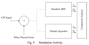
To validate the functionality of the proposed algorithm, simulation activity has been carried out. By using MatLab environment the two DDC architectures, traditional and parallel, have been implemented and fed with the same input signal; then a comparison analysis of the outputs has been performed. The validating concept is shown in Figure 9.
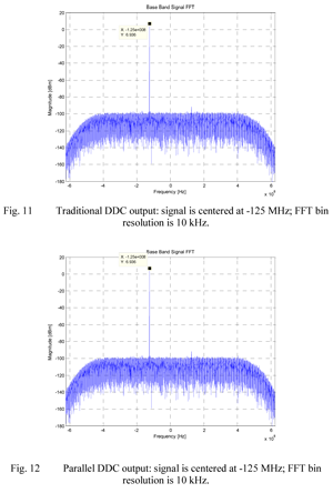
As input, a CW signal with thermal noise is used. According to our case study, the carrier frequency is contained in the band [500÷1000] MHz after the 5 GSps ADC sampling. NCOs are locked at a frequency of 625 MHz. The FIR with the frequency response shown in Figure 7 has been used in traditional DDC, and starting from it the FIRs used in the parallel architecture have been calculated. The architecture emulates a FPGA working at 312.5 MHz, providing I and Q signal at 1.25 GSps.
Figure 11 and Figure 12 show respectively traditional DDC output and parallel architecture output.
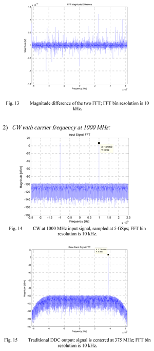 In Figure 13 the magnitude difference of the two FFT outputs is reported. The figure shows how the two architectures, traditional and parallel, actually give the same results.
For sake of brevity, only two cases are reported in this paper, but several simulations were performed for different CW inputs in the frequency band of interest and, for all of them, traditional and parallel DDC have given the same results.
V. Innovative DDC Design Using Xilinx System Generator
Hardware implementation of the proposed algorithm has been realized using System Generator, a High Level Synthesis Tool (HLS) provided by Xilinx.5 Vivado HLS has been used to evaluate FPGA resources utilization, power dissipation and meeting of timing constrains.
The target FPGA is the Xilinx FPGA Kintex7 XC7K325T2FFG900C.
Figure 18 shows the System Generator design for the parallel architecture, the design is in accordance with the case study proposed in this paper, considering a fFPGA of 312.5 MHz and 8 data streams as outputs (4 streams for I components and 4 streams for Q components). Processing delay (i.e. first sample in–first sample out) is of the order of tens of samples at 312.5 MHz. 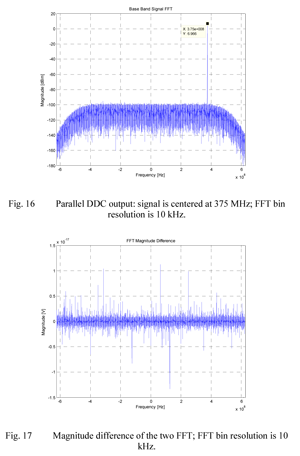
Resources employment of the target FPGA is shown in Table 1.
| Utilization | Utilization % | |
| LUT | 12468 | 6 |
| LUTRAM | 6000 | 9 |
| FF | 27392 | 7 |
| DSP | 592 | 70 |
| BUFG | 1 | 3 |
Vectorless power estimation method6 has been used to estimate power dissipation of the proposed architecture. Furthermore ambient temperature at 50°C, maximum process, nor airflow neither heatsink have been considered. Results are shown in Figure 19.
Implementation of the proposed algorithm into the selected FPGA is shown in Figure 20; FPGA timing analysis gave the results shown in Figure 21. 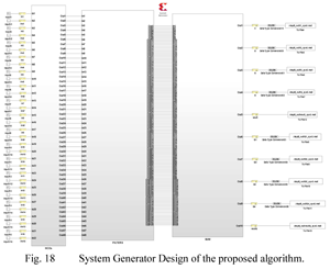
VI. Conclusions
Thanks to the proposed parallel architecture, it is possible to process wide band signals with clock elaboration frequency lower than the one required by Nyquist theorem, making it possible to use commercial FPGA for real-time processing.
Such an architecture is a key solution for RADAR using wide band fully digital receiver, where super-heterodyne is no longer existing: 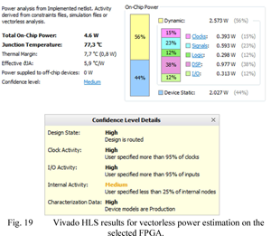 parallel architecture can be used as digital front end for wide band DDC (processing the whole operative bandwidth), then digital tuning and decimation can be applied to extract the desired instantaneous signal bandwidth.
Furthermore, thanks to the capability of managing wide band signals, this architecture can also be used for communications and electronic warfare applications. 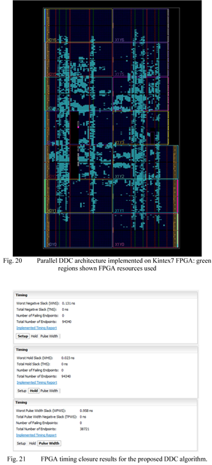
References
- U. Jayamohan, "Not Your Grandfather’s ADC: RF Sampling ADCs Offer Advantages," 2015.
- "RF Sampling S-Band Radar Receivers," Texas Instruments Design, 2016.
- J. G. Proakis and D. K. Manolakis, "Digital Signal Processing: Principles, Algorithms and Application," 4th Edition, Pearson, 2006.
- "Mixed-Signal and DSP Design Techniques," Analog Devices, 2002.
- "Model-Based DSP Design Using System Generator, UG897," Xilinx, 2016.
- "Power Analysis and Optimization, UG907," Xilinx, 2015.