
Bottom termination components (BTCs) have become one of the most common packages with the highest growth rate. Typical assemblies now have many of these components, often with varying types of BTCs on one assembly. What can be done when one or more BTCs start to show increased variation within the same process? Investigations have been conducted to find materials that offer the lowest voiding in large ground plane solder joints. In addition, process modifications have continually been proposed to help alleviate voiding in BTC components. These include but are not limited to: pad design, pad patterning, stencil design, via positioning, solid solder addition, and reflow profile optimization.
Improved pad design strategies have been proven in the industry. IPC committees are updating recommendations for design and implementation of BTCs, including major changes to IPC-7093. This article will discuss these changes and how these strategies can be used to minimize voiding and ensure robust BTC assemblies.
Introduction
Defining BTCs:
Bottom termination components are also known by other names in the electronics industry such as QFN, SOIC, LGA and many more. The defining characteristic is that all of the terminations are flat on the bottom of the component, relying only on solder paste to make the component to board connection. These components do not have a solder ball, as BGAs do. This means that the standoff height is entirely determined by the volume of solder. The resulting assembly has no visible solder joints, unless the component features wettable flanks, which are not required. This makes BTCs more challenging to inspect, often leading to X-ray analysis for process control.
From a reliability standpoint, BTCs have very long lifetimes in thermal cycling and drop testing1. This is usually attributed to their sturdy construction, with a large central solder joint and smaller I/Os along the edges. Testing has even showed good reliability with voiding up to or exceeding 50% of the area of the thermal pad.
Industry organizations have published guidelines for assembling these components. They can be quite cumbersome and difficult to follow due to the variety of these components. IPC-7093 was first published in March 2011 and is currently undergoing an overhaul of content to incorporate further best practices, developed and learned over the last decade of BTC component use.
Some BTC components have requirements that go above and beyond the scope of this paper. High voltage or frequency requirements, sensor technologies, and asymmetrical BTCs often will have special assembly instructions that are critical to function. Assembly recommendations from the component supplier should be carefully reviewed in addition to industry standard guidelines.
Assembly Challenges:
There are three ways that the assembly of a BTC can lead to failure: shorted or missing I/O connections, insufficient standoff height, or excessive voiding. Any imperfections in the I/O connections will lead to functional failure of the component. Most commonly, the I/O connections will be compromised due to tilting of the component; either from variations in placement, especially with systems that rely solely on z-height measurement or due to the surface tension of the molten central paste deposit causing the component to float during reflow. Insufficient standoff height can be the result of too little paste, or more commonly, solder being displaced into plated vias. Solder joints that are thinner, with less standoff height, may be less robust and more prone to crack propagation. Voids within areas with low standoff can contribute more frequently to the failure mechanism.
Voiding under bottom terminated components (BTCs) is a major challenge for the electronics industry, although not because of voids’ impact on solder joint reliability. Poor thermal conductivity results from discontinuity in the z-axis of the solder joint due to voids. In BTCs with high power requirements, initial assembly testing will assure functionality and continuity on the signal leads; however, in some cases this does not prevent field failures. These costly-to-fix failures can often be attributed to poor thermal conductivity in the center solder joint leading to overheating and die-cracking.
Inspecting BTCs can be challenging because there are concealed solder joints, requiring X-ray scans of the assemblies. X-ray imaging gives a 2-dimensional view of the component and designates lower density areas with a lighter contrast (see Figure 1). Software is then used to quantify the % of the area that shows voids, the size of the largest void, and total number of voids. It is also important to look at the images of perimeter solder joints as bridges can be detected and varying shapes can sometimes indicate variations in component co-planarity. Components with voiding are typically reliable and it is only in a minority of components that voiding will lead to failure. Nonetheless, since voids are very apparent on X-ray analysis, the endeavor to eliminate them will continue.

Figure 1. QFN voiding X-rays showing examples of minimum and maximum values with analysis.
Optimizing an assembly process to minimize voiding will mean looking more closely at many aspects of the assembly. Minimum voiding is not easily achieved by changing one part of the process or simply switching solder materials. Many different assembly scenarios have been investigated when voiding has played a part in failures. The contributing factors are varied and are grouped into three types: design, process, and material. These are shown in Figure 2.

Figure 2. Illustration of the factors contributing to successful BTC assembly
Two primary mechanisms contribute to void formation: poor wetting and volatile entrapment. First, areas that do not allow the solder to wet well will cause inconsistency in solder joint formation and increase the probability for voiding. Poor wetting is often caused by deterioration of the surfaces of components and pads. Surface finishes protect copper pads from oxidation in contact with air. They also serve as a barrier to solder joint formation because the flux or metallurgy must form a bond despite the presence of the surface finish. In this way, surface finishes can vary greatly in their impact on voiding. Solder paste flux works to remove oxides and enhance wetting.
Volatile entrapment, the second mechanism, is uniquely challenging with BTCs because of the large covered area and low standoff between the components and the board. During reflow, board and solder materials that contain volatile compounds will outgas. These gases freely escape around other components because they are not constrained by the tight spacings found in BTCs. Once liquidus is reached in reflow and the solder alloy melts to form the solder joint, any remaining entrapped gas can form bubbles. Many of these bubbles are pushed to escape by the surface tension of the liquid solder, but those that do not escape before the alloy solidifies will be present in the solder joint as voids.
While focused on voiding, it is easy to lose sight of the most critical factor in assembling BTCs: standoff height. Component manufacturers recommend a certain amount of standoff provided by the solder joint. Component manufacturers recommend that the minimum acceptable standoff is around 50 microns. This is typically measured through destructive analysis such as cross-sectioning and using SEM imaging for measurement.
The cross-sectional images in Figure 3 show a worst-case example with open-plated vias. The standoff height is reduced to 35 microns and the solder on the perimeter solder joints has been squeezed out. The external bumps of solder form an interior corner at the edge which will contribute to crack propagation. The vias in this design are intended to aid in conducting heat from the component die. There are several different designs for thermal vias; typically they are plated through holes, sometimes with a plug or barrier on top to discourage solder from wicking into the vias. When solder can flow into the vias, a considerable portion of the solder volume is displaced, leading to insufficient standoff height.

Figure 3. Worst-case example of solder escaping into vias, reducing standoff height
Some X-ray equipment is now capable of topographical analysis that can detect height and co-planarity. In most cases, the component will be tilted if there is a displacement of solder into vias. This can be a powerful tool in identifying components more prone to field failures. If the solder joint is less than this minimum thickness, there will not be enough solder to bridge the gap for CTE mismatches between the board and component. This can lead to additional functional failures with only a tenuous link to voiding.
Solder joints with sufficient standoff have shown acceptable performance in accelerated life testing with voiding up to 50%. This does not take into account the thermal load required for the component to function optimally, but does demonstrate the robust nature of the solder joints associated with BTCs.
Case Study of Factors Contributing to Voiding:
Surface Finish and Component Cleanliness
Investigating the impact of surface finish on the boards and components is critical because it contributes greatly to the function of solder wetting and variations in voiding performance. In this case, we studied the voiding for one solder paste, one component design, and one board design, while varying surface finish and level of oxidation.
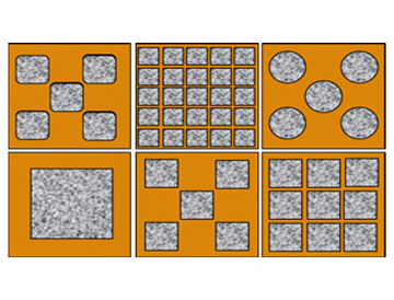
Figure 4. Test board design with QFNs and window-pane stencil design
This design uses a commercially-available dummy QFN with a tin finish. Since components are placed only on five locations in Figure 4, it is possible to see how the solder has wet to the central pad and perimeter pads. The stencil design is broken into quadrants to minimize component floating during liquidus and to form channels to encourage volatile escape. These boards were tested with four surface finishes: ENIG, OSP, immersion silver (Ag), and immersion tin (Sn). Some boards were also tested in an oxidized condition, achieved by sending the boards through the same reflow profile twice before printing the solder paste and reflowing again.

Figure 5. Results of surface finish comparison testing
In Figure 5, mean lines in each box show that the oxidation of the boards played little role in voiding differences (less than 1% difference compared to a spread of data around 30%). ENIG boards had increased variation. The diamond plots summarize the scatter of data points to show the mean and represent the variation. The ENIG finish corresponded with higher amounts of voiding, which is an unexpected result. Typically the ENIG finish is chosen to be the best oxygen barrier.
Stencil Design
When discussing the need to have enough solder volume for a robust solder joint, it is necessary to consider stencil design. The first priority is to calculate the appropriate volume of solder paste on the perimeter solder joints. Too much solder here can contribute to bridging, while too little can increase the propensity for the component to tip. Perimeter pads should not extend past the edge of the component, especially if there are not plated leads (wettable flanks) along the edge. Next, the focus is sizing and distributing solder deposits to fill the central pad. It is most common to print several deposits on this pad for two reasons: to minimize lifting or floating of the component due to the surface tension of molten solder and, secondly, to keep solder from flowing into vias.
Component manufacturers often recommend designs as illustrated in Figure 6, which suggest area coverage between 37% and 81%. Considering that area reduction geometrically, it seems logical that voids would emerge as the volume of solder is less than the theoretical space to be filled.


Figure 6. (a.) Recommended stencil designs from component manufacturer guidelines; (b.) stencil design for test design and geometric values
Continuing on this path of logic that solder paste volume should be adjusted to assure sufficient solder alloy to fill the expected volume of the solder joint for appropriate standoff, stencil designs were chosen to vary area coverage and resulting solder alloy volume. These stencil designs were tested2 with a 4 mil foil as well as a 5 mil foil to give an apples-to-apples comparison of a clear 25% increase in solder paste volume. The table in Figure 6 shows calculations for each stencil design. This assumes a 50 micron standoff for the full pad as theoretical volume.
Figure 7 compares the results of two solder pastes; one is optimized for low-voiding and the other is a legacy benchmark material. Paste A clearly shows less voiding overall and less variation. The different stencil designs do not have a large impact on the overall voiding percent. When comparing the stencil thickness, the 4 mil designs seem to have slightly more variation. Paste G shows a higher average and more variation overall. The full pad design yields a slightly lower average, but there is little difference between designs. The 5 mil stencil seems to have more variation, but also has some very low values. Discussion of these results has led to two hypotheses: component cleanliness plays a significant role in the incidence of high values, and/or another factor such as placement height contributes significantly in the case of pastes with a propensity for void formation. This second hypothesis reinforces the importance of standoff height, not only after reflow, but also after placement. It should also be noted that these results would likely show greater improvement if the board design included vias or solder mask patterning to match the stencil designs.3
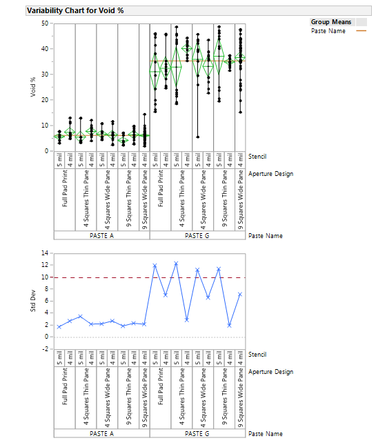
Figure 7. Results from stencil design investigation
Material Selection
Solder paste is comprised of powder with a chosen alloy composition and flux. The ratio of metal to flux, typically expressed as metal loading by weight, can affect voiding. Higher metal loadings can be favorable because the thicker paste maintains more standoff height during preheat. Decreasing powder sizes can pose a challenge due to increased surface area of oxidation. In addition, some solder alloys intrinsically have different voiding performances because of differences in wetting characteristics, surface tension, and oxidation resistance. On the other hand, there are several aspects of flux that can contribute to voiding under BTCs: how strongly the flux prevents oxidation and promotes wetting, and how the flux volatiles evolve during reflow. Solder pastes specifically designed to reduce voiding often achieve this with trade-offs in other areas of performance, such as stability or printing performance.
Referring again to Figure 7, this is a typical material comparison. All process and design factors should be kept constant aside from solder paste selection. Often the comparison is conducted at more than one reflow profile to allow for process preferences, or in this case, different stencil designs. The difference between Pastes A and G is quite pronounced; typically, one material will not show such a dramatic improvement.
Addition of Solid Solder Preforms
In many cases, especially for designs with open vias, it might not be possible to stencil print enough solder paste to supply the solder volume needed. Solid solder preforms can be used to add solder volume without adding flux volatiles. There are two prevailing strategies here: use a preform that is thin and flat with dimensions slightly smaller than the central thermal pad and place it into the paste3, or use a preform in a standard size similar to a 0402 component, which will tilt the component temporarily, but coalesce completely during reflow4.
Reflow Profiling
Reflow profile optimization is often a first go-to solution due to the ease of modification. Different materials may have different unique preferences, but there are some trends that impact voiding performance2:
- If the preheat is too quick, there is not enough time for volatiles to evolve and escape before the solder is molten
- If the preheat is too quick, the paste can slump, reducing the standoff and preventing the escape of volatiles
- If the profile is generally too short, volatiles will be more easily entrapped
- Low peak temperature tends to require more time for complete solder wetting
- Excessive peak temperature or profile length results in oxidation on surfaces, increasing the potential for voiding
- Reflow in nitrogen leads to lowest voiding results (aside from vapor phase, or vacuum reflow processes)
Investigations have often shown that voiding can be minimized with a longer or hotter profile. However, these investigations are typically conducted with a focus only on BTCs. It is important to always consider the full assembly when profiling. For production assemblies, the process window will be limited by several factors: component maximum temperatures, oxidation resistance on large components, avoiding graping on small components, etc. When creating an optimal profile for voiding on a production assembly, profiling to minimize voiding must be tempered with attention to the other challenging parts on the assembly.
Design Solutions for Tomorrow’s BTC Goals
Process optimization can achieve the goals associated with today’s component designs. The next generation of discussion about BTCs centers on improving the design criteria to meet the goals of BTCs with higher requirements. Whether these requirements are based on high voltage, frequency, or thermal demands, process optimization falls short of solving the problem. Shrinking package sizes also raise the bar on the challenge of assembling the next generation of BTCs.
Industry leaders have already developed some solutions to this problem. The main focus is to keep solder away from open vias where vias cannot be plugged. These strategies, such as Via-in-Pad Plated Over (VIPPO)5, allow for inclusion of vias in shrinking geometries without compromising solder volume. Also, these designs limit variations in voiding and component tilt.

Figure 8. Pad design and stencil design for optimal BTC assembly reliability (Courtesy of Tom Hauscherr and Matt Kelly, IBM)
The design in Figure 8 will be one of the most intriguing additions to the next revision of IPC-7093. This design uses open vias for thermal management, but also keeps solder away by using a pattern of solder mask. This solder mask patterning6 was investigated early in the adoption of BTCs as a strategy for maintaining outgassing pathways. Further design options are detailed in Figure 9.

Figure 9. BTC Thermal Pad Design Options
The challenge with QFN printed circuit design is balancing assembly/rework, power, thermal, and signal integrity requirements to sufficiently dissipate heat and electrical current while ensuring the device is easily manufacturable. Factors to consider when specifying thermal via design are compared in Table 1, below7.

Table 1. Design Option Pros and Cons from new revision of IPC-7093
Conclusions
There are many factors to consider when preparing to assemble circuit boards with BTCs. Process and material choices can be critical in avoiding conditions that will lead to inconsistency in the robustness of the solder joints, whether this variation comes from decreased standoff height, component tilting, or high levels of voiding. Board design including via considerations is increasingly more important, as some design choices intrinsically lead to assembly challenges.
Through development of the new revision of IPC-7093, one thing has been clear: there are many variations on pad/via designs, more numerable than names for BTCs. Some choices can lead to decreased standoff height or large amounts of voiding, which can sometimes be attributed to field failures. Best practices have been determined to lead us away from these well-learned pitfalls, but successful BTC assemblies must originate at the design phase.
References:
- BTC Voiding: Component and Solder Joint Reliability. Rockwell Collins. Hillman. SMTAi 2016.
- How Stencil Design and Reflow Profiles Affect Variation in QFN Voiding Data: A Case Study. Indium Corporation. Sandy-Smith. SMTA ICSR 2016
- Minimizing Voiding in QFN Packages Using Solder Preforms. Indium Corporation. Homer, Lasky. SMTAi 2011.
- Voiding Control Beneath BTCs Using Solder Fortification® Preforms. Indium Corporation. Herron, Luo et al. SMTAi 2015.
- Via-in-Pad Plated Over (VIPPO) Design Considerations for Enterprise Server and Storage Hardware. IBM Corporation. Kelly, Jeanson et al. SMTAi 2015.
- The Effect of Thermal Pad Patterning on QFN Voiding. Indium Corporation. Lee, N.C., et al. APEX 2012.
- IPC-7093. March 2011 and future revision to be released.