
The promise of 5G new radio technologies to provide significant improvements in throughput, super low latency and reliable, ubiquitous coverage is critically based on the availability of new spectrum. The 3GPPP group has identified new spectrum both below and above 6 GHz in a drive toward global harmonization. The future 5G ecosystem will most likely feature macro base stations transmitting in spectrum below 6 GHz for physical coverage, while mmWave frequencies will be used for capacity enhancements.
The frequency band from 3400 to 3800 MHz has generated wide interest due to its potential to be available on a global basis, having already been identified for mobile communications use in many European countries, in China (which includes frequencies down to 3300 MHz) and in the U.S. RF characteristics at 3.5 GHz make this band suitable for use in both massive MIMO systems with beamforming antennas and in more traditional cellular base station architectures. ITU identifies these 3.5 GHz frequencies as band 42 (3400 to 3600 MHz) and band 43 (3600 to 3800 MHz).
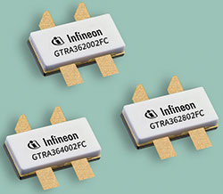
THREE NEW DOHERTY TRANSISTORS
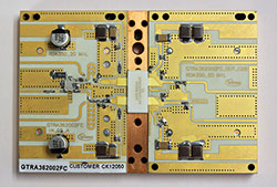
Figure 1 The GTRA362002FC is an asymmetric transistor delivering more than 200 W of combined peak output power.
Many field trials are underway in the 3.5 GHz bands. To address this market, Infineon has developed a line of GaN on SiC RF power transistors for Doherty amplifier applications that are capable of the highest efficiency and broadband operation. GaN on SiC technology has stormed the cellular RF power market in recent years due to its high-power density and high efficiency. These characteristics enable designers to create highly compact amplifier circuits with more than a 10 percentage point improvement in efficiency above 3 GHz, compared to LDMOS solutions, and wideband performance that facilitates the design of Doherty amplifiers.
These transistors are matched for optimal operation between 3400 and 3600 MHz, the band with the most global availability. One of the challenges at this band is the wide signal bandwidth of 200 MHz. To facilitate the design of a wideband Doherty and to compensate for the changing input impedance of the peak amplifier over power (running at class C), special attention was placed on the design of the internal transistor input match, with techniques developed to enhanced wideband operation while leaving the output unmatched. Further, these transistors use an asymmetric design for better efficiency with high peak-to-average ratio (PAR) signals.
The GTRA362002FC is an asymmetric transistor with more than 200 W of combined peak output power, designed for amplifiers in 20 W cellular systems. It has two outputs: the carrier or main side with 85 W output power and the peak side with 115 W of P3dB output, for a split ratio of 1:4. Infineon developed a Doherty reference design that provides 14 dB of gain, 45 percent drain efficiency and ‐29 dBc adjacent channel power ratio (ACPR), measured with a single carrier WCDMA, 10 dB PAR signal at 3600 MHz and 29 W average output power (see Figure 1).
The GTRA362802FC is also an asymmetric design. Offering more than 300 W of combined peak output power, it is targeted at 30 W cellular systems. It provides 115 W on the main side and 170 W on the peak side of a Doherty. With a single carrier WCDMA, 10 dB PAR signal at 3600 MHz and 44 W average output power, a Doherty amplifier reference design is capable of 14 dB of gain, 49 percent efficiency and ‐31 dBc ACPR. Typical Doherty performance of the GTRA362802FC is shown in Figure 2 (Pout, efficiency and gain) and Figure 3 (gain and efficiency versus frequency).
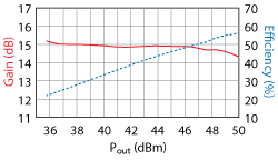
Figure 2 Typical Doherty output power, efficiency and gain of the GTRA362802FC at 3500 MHz. The transistor is biased at VD = 48 V, IDQ (main) = 140 mA and VGS (peak) = −5.3 V.
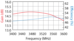
Figure 3 Typical Doherty gain and efficiency vs. frequency of the GTRA362802FC. The transistor bias is the same as for Fig. 2.
The higher power GTRA364002FC has been designed for use in 40 W cellular systems and provides more than 400 W of combined peak output power. Its main side outputs 170 W at P3dB and the peak side 255 W, for a 1:5 power split ratio. Using a single carrier WCDMA, 10 dB PAR signal at 3600 MHz and at 59 W average output power, the Doherty reference design is capable of 13 dB of gain, 43 percent efficiency and ‐30 dBc ACPR.
All devices are available in an open cavity, ceramic lid package with CPC flange. Thermal resistance for these transistors ranges from 1 to 1.7°C/W (measured at Tcase = 75°C and CW signals using an infrared measurement). Engineering samples are available, as well as a reference Doherty amplifier for each product; volume production is planned for the end of 2017.
Infineon Technologies
El Segundo, Calif.
www.infineon.com/rfpower