
A bandpass filter (BPF) design using double-sided edge-coupled microstrip lines and stepped impedance stubs features intrinsic transmission poles, beneficial for achieving an ultra-wide bandwidth. When shunted with stubs of different length ratios, multiple transmission zeros are introduced, yielding sharp band edges, deep out-of-band attenuation and high in-band return loss. Experimental results show in-band return loss greater than 16 dB from 3.1 to 10.6 GHz and out-of-band attenuation of 34 dB and 18 dB for the lower and upper stopbands, respectively, while the band edges are very sharp.
wing to its unique advantages—very high data rates, less power frequency density, interference immunity and suitability for covert communication—ultra-wideband (UWB) (3.1 to 10.6 GHz) technology has been employed in many applications since the frequency band was licensed by the U.S. Federal Communication Commission in 2002.1 The stringent frequency mask requirement, however, is a challenge for the design of an UWB BPF. It must have good return loss, low insertion loss, sharply sloped band edges and deep stopband attenuation.
Several design techniques have been used. The stepped impedance resonator, a type of multi-mode resonator (MMR), is good for achieving a wide passband.2 It is made up of a half wavelength transmission line of characteristic impedance Z1 placed between two quarter wavelength lines of characteristic impedance Z2. In an UWB BPF design, Zhu et al.,3 demonstrated an ultra-wide passband from 2.96 to 10.67 GHz; however, the band edges were not sharp.
Several subsequent modified MMR techniques that added open and/or short-circuited stubs increased the roll-off rate to some extent,4-7 yet the stopband rejection was not satisfactory and the passband return loss was poor. The size of the MMR is large because it is at least one wavelength long. Other techniques such as the use of a multi-layer broadside coupling structure8 and a ring resonator shunted with a grounded stub9 have also been studied but exhibit gradual roll-off characteristics as well.
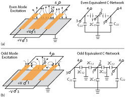
Figure 1 Electric field distributions and equivalent capacitance networks for the even (a) and odd (b) modes.
In this article, the double-sided edge-coupling structure loaded by stepped impedance stubs is utilized. This is similar to the approach taken by Singh et al.,10 but with one more stub and the incorporation of bent stubs with different length ratios. With loading of the fourth stub and different length ratios, more transmission zeros, deeper rejection in the stopband, sharper band edges and better in-band return loss is observed.
DOUBLE-SIDED EDGE-COUPLED LINE MODEL
The double-sided edge-coupled line is also referred to as a three-line transmission line with six ports.11 If the ends of the two side lines are connected, a four-port network is obtained and even/odd mode analysis can be applied. Figure 1 shows the electric field distributions for even and odd mode excitations. The deduction of the equivalent capacitance networks (C-network) is similar to the single-sided case described by Pozar.12
An even mode is excited when the sources added on ports 1 and 3 are in phase; a magnetic wall occurs in the gap between the center and either side conductor. As no E-field goes across the gap, the equivalent C-network is composed solely of self-capacitances (C11 and C22). However, when sources on ports 1 and 3 are out of phase, an electrical wall occurs and a voltage null appears in the gap. So, in addition to self-capacitances, symmetric mutual capacitances (C12) shunted to ground are included to account for the effects.
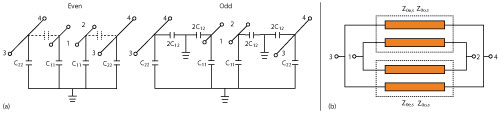
Figure 2 The split form equivalent C-network (a) and the resulting transmission line model (b).
The C-networks in Figure 1 can be transformed into the split form in Figure 2a, or the merged form in Figure 3a. These two new C-networks give rise to models in which the more commonly used single-sided coupled line model is configured in two different topologies:
1. Two coupled lines with characteristic parameters Z0e,s and Z0o,s, as shown in Figure 2b, are stacked to compose a four-port network for the resulting model of the split form.
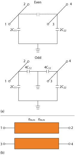
Figure 3 The merged form equivalent C-network (a) and the resulting transmission line model (b).
2. As shown in Figure 3b, one coupled line model with characteristic parameters of Z0e,m and Z0o,m is the result for the merged form.
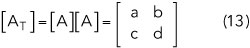
The even and odd capacitances of each C-network are:
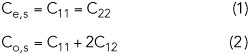
for the split form, and
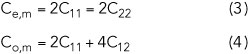
for the merged form.
The even and odd mode characteristic impedances of each single-side coupled line in the resulting transmission line model are:
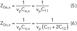
for the split form, and
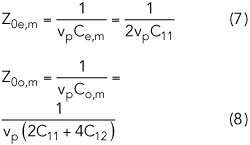
for the merged form. The phase velocity vp is assumed equal for even and odd modes.
Notice that the models transforming Figure 1 to Figure 2 and Figure 1 to Figure 3 are equivalent. There are two assumptions behind this: The self-capacitance of the center conductor is twice that of the side conductor in Figure 1, so the center is wider. The mutual coupling between the center line and either side in Figure 1 is assumed equal to that of the single-sided coupled line in Figure 2b and half that of the one in Figure 3b.
From Equations 5 to 8, the relationships between the characteristic impedances of the two forms are
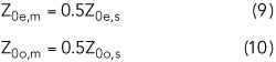
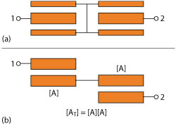
Figure 4 Double-sided (a) and single-sided (b) edge-coupled line equivalence.
FILTER DESIGN
The equivalent models derived above can be used to facilitate the filter design. For example, a cascaded two stage, double-sided, edge-coupled transmission line model can be simplified to a single-sided model as shown in Figure 4.
The Z matrix of one single-sided coupled line is given by Pozar.12
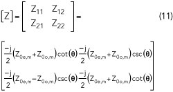
in which θ is the electric length.
Deriving the ABCD matrix using Z elements gives
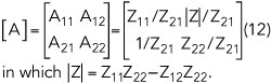
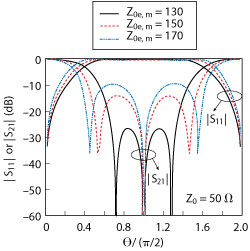
Figure 5 S-parameters of an ideal two stage circuit. Z0 = 50 Ω (not necessary but used for simplicity).
Then the total ABCD matrix and the S-parameters of the two stage circuit can be found by
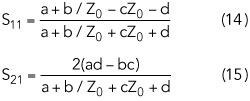
If we let Z02 = Z0e,m*Z0o,m and solve for θ when S11 = 0, we find three transmission poles in the passband:
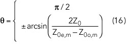
A real solution of θ is obtained when Z0e,m – Z0o,m ≥ 2Z0. The number of poles in the circuit in Figure 4 is the same as what a stepped impedance MMR can provide by itself,3 which increases if more stages are cascaded. Example S-parameters of the two stage circuit are shown in Figure 5.
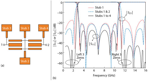
Figure 6 Two stage circuit (a) and modeled S-parameters vs. number of shunted stubs (b).
The next step is to shunt the stepped impedance stub to increase the roll-off rate. It is convenient to control the transmission zeros by tuning the impedance ratio of the stub.10 If we locate the first zero to the left edge of the passband and the second to the right, sharp edges can be obtained. Using the coupled line model above, we can quickly obtain the theoretical performance with stubs as shown in Figure 6. There are three cases, according to the number of stubs used. Case 1 is a single stub (1). Case 2 contains two stubs with the same length and impedance ratio, so that there is only one transmission zero beside each edge, which is the same as for case 1. For case 3, stubs 1 and 2 are different, and stubs 3 and 4 are the same but different than either stub 1 or 2, so that there are three transmission zeros beside each edge. It can be seen from Figure 6 that with more stubs shunted and with the impedance ratio varied, not only the roll-off rate but also the out-of-band attenuation increases. The in-band return loss increases as well.
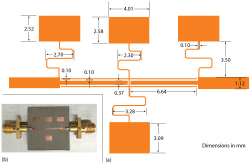
Figure 7 The circuit configuration (a) and fabricated filter (b). Dimensions in mm.
MEASURED RESULTS
To verify the analysis, an UWB BPF was simulated and then fabricated. The chosen substrate was the popular low-cost RF-35 with a dielectric constant of 3.5 and a thickness of 0.508 mm. The filter (see Figure 7a) consists of two cascaded double-sided coupled lines and four shunted stubs with three different length ratios (stubs at two sides are mirrored to each other). The coupled line is a quarter guided-wavelength long at the center frequency of 6.85 GHz, so that the length of this filter is about half that of an MMR based UWB filter.
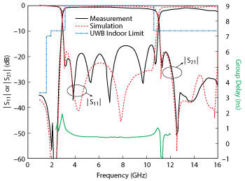
Figure 8 Measured results compared with simulation and the UWB indoor frequency mask.
To locate the transmission zeros beside the edges, we adjusted the length ratio of the stubs rather than impedance ratio, because it is more convenient to vary the length of the line without enlarging its size. HFSS was used to optimize the overall performance. Compared to the design by Singh et al.,10 this design has one more shunted stub located in the center (below the through line) to increase out-of-band attenuation and band edge selectivity. All the stubs are bent to reduce size. Figure 7b shows the assembled filter.
As seen from the measured results in Figure 8, a passband with return loss greater than 16 dB is achieved from 3.1 to 10.6 GHz. Insertion loss, including the connector, is less than 1 dB from 3.1 to 10 GHz. The roll-off rate is very high at both lower and upper band edges. Out-of-band attenuation is greater than 35 dB in the lower stopband and greater than 18 dB in upper stopband, which satisfies the UWB indoor requirement. Meanwhile, the group delay is flat and less than 0.5 ns. Measured results agree well with simulation and are consistent with the design prediction.
CONCLUSION
An UWB BPF using a double-sided edge-coupling structure and shunted stepped impedance stubs is shown to be well suited for achieving ultra-wideband performance. With shunted stubs, transmission zeros at both the lower and upper band edges are introduced to increase selectivity and out-of-band attenuation. Measured results show good agreement with simulation and validate the design analysis.n
ACKNOWLEDGMENT
This work was supported in part by the Major Project of Scientific Instrument and Equipment Development approved by Ministry of Science and Technology (MOST) of China under Grant 2013YQ200503. Xin Feng would also like to thank the China Scholarship Council for supporting his studies in the U.S.
References
- “Revision of Part 15 of the Commission’s Rules Regarding Ultra Wideband Transmission Systems,” FCC, Washington D.C., 2002.
- Y. C. Chiou, J. T. Kuo and E. Cheng, “Broadband Quasi-Chebyshev Bandpass Filters with Multimode Stepped-Impedance Resonators (SIRs),” IEEE Transactions on Microwave Theory and Techniques, Vol. 54, No. 8, August 2006, pp. 3352–3358.
- L. Zhu, S. Sun and W. Menzel, “Ultra-Wideband (UWB) Bandpass Filters Using Multiple-Mode Resonator,” IEEE Microwave and Wireless Components Letters, Vol. 15, No. 11, November 2005, pp. 796–798.
- S. W. Wong and L. Zhu, “Quadruple-Mode UWB Bandpass Filter With Improved Out-of-Band Rejection,” IEEE Microwave and Wireless Components Letters, Vol. 19, No. 3, March 2009, pp. 152–154.
- Q. X. Chu and X. K. Tian, “Design of UWB Bandpass Filter Using Stepped-Impedance Stub-Loaded Resonator,” IEEE Microwave and Wireless Components Letters, Vol. 20, No. 9, September 2010, pp. 501–503.
- H. W. Deng, Y. J. Zhao, L. Zhang, X. S. Zhang and S. P. Gao, “Compact Quintuple-Mode Stub-Loaded Resonator and UWB Filter,” IEEE Microwave and Wireless Components Letters, Vol. 20, No. 8, August 2010, pp. 438–440.
- H. Zhu and Q. X. Chu, “Compact Ultra-Wideband (UWB) Bandpass Filter Using Dual-Stub-Loaded Resonator (DSLR),” IEEE Microwave and Wireless Components Letters, Vol. 23, No. 10, October 2013, pp. 527–529.
- A. M. Abbosh, “Planar Bandpass Filters for Ultra-Wideband Applications,” IEEE Transactions on Microwave Theory and Techniques, Vol. 55, No. 10, October 2007, pp. 2262–2269.
- W. Feng, W. Che and Q. Xue, “Compact Ultra-Wideband Bandpass Filters with Narrow Notched Bands Based on a Ring Resonator,” IET Microwaves, Antennas & Propagation, Vol. 7, No. 12, September 2013, pp. 961–969.
- P. K. Singh, S. Basu and Y. H. Wang, “Planar Ultra-Wideband Bandpass Filter Using Edge Coupled Microstrip Lines and Stepped Impedance Open Stub,” IEEE Microwave and Wireless Components Letters, Vol. 17, No. 9, September 2007, pp. 649–651.
- J. T. Kuo and E. Shih, “Wideband Bandpass Filter Design with Three-Line Microstrip Structures,” IEEE MTT-S International Microwave Symposium Digest, Vol. 3, May 2001, pp. 1593–1596.
- D. M. Pozar, Microwave Engineering, John Wiley & Sons, 2009.