
A PA Driver for Split-band PCS Applications
RF Micro Devices Inc.
Greensboro, NC
Due to the growing popularity of PCS systems, there has been an increasing demand for high performance RFICs for the PCS band. The transmit and receive frequencies for the PCS band are allocated at 1850 to 1910 MHz and 1930 to 1990 MHz, respectively. When a mobile handset is transmitting, the close proximity between the transmit and receive bands causes receive interference and, consequently, increases the noise power in the receiver. To reduce noise power and improve isolation, most transmitter system designs use surface acoustic wave (SAW) filters between the PA driver and the PA. However, a typical SAW filter centered at the PCS transmit band only offers approximately 15 dB receive band attenuation. This low attenuation causes considerable transmitter noise interference in the receiver front end. To alleviate this problem, system designers have been using split-band filters. A split-band filter uses two SAW filters (one for the lower half of the transmit band and another for the higher half of the band) and provides greater than 30 dB receive band attenuation.
 The model RF2351 high performance power amplifier (PA) driver is specially designed to interface with such split-band filters by providing two switched outputs to interface with the split-band filters in the transmit chain of a PCS system. Figure 1 shows a block diagram of a typical RF2351 application.
The PA Driver
The RF2351 RFIC is a high performance, low cost PA driver. The IC is designed using the company’s proven GaAs heterojunction bipolar transistor (HBT) technology and is housed in a small 4 x 4 MLF16 package. The four-sided MLF16 package provides good isolation between the two outputs. The architecture of the PA driver comprises two common emitter amplifier stages. The bias control circuits generate the appropriate bias to control the collector currents, and the amplifier operates in class A mode. Interstage matching is achieved by using an internal capacitor and external inductor. The input impedance is set by the combination of this inductor and the residual emitter inductance. The input is DC blocked externally using a 22 nF capacitor, and the output impedance is set by a simple external LC match.
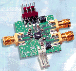
 Moving most of the gain to the final stage improves linearity, thus more than half of the total gain is provided by the second stage. However, decreasing the gain at the first stage deteriorates the noise figure. These trade-offs were balanced very carefully through computer simulation to achieve optimum performance. The simplified circuit topology for the PA driver is shown in Figure 2 . Figure 3 shows the device block diagram with the application circuit used on the evaluation board; Figure 4 shows the device mounted on the evaluation board. The second stage ground is connected to the die paddle. Since the part uses an exposed die package, care must be taken to ensure that the exposed metal at the bottom makes good electrical contact with the PC board. Aside from its standard features, the RF2351 also offers various other functions such as power control and current adjust.
 When not in use, the RF2351 can be shut down by grounding the Vpd pin. In this state the IC will draw less than 10 µA, eliminating the need for a supply-side switch. By adjusting the voltage applied to the Vpd pin the user can control the bias current and thus the total current (Icc ) consumed by the part.
The first stage ground is brought out through pin 4 to provide external degeneration. Any inductance connected to this pin provides negative feedback. Raising inductance at pin 4 increases the input impedance, lowers the gain and noise figure, and improves linearity. This capability allows the designer to fine-tune key parameters to suit a particular application.
 The Osel pin toggles the outputs. When it is set between 2 and 3.5 V, OUT1 is selected and the 0 to 0.4 V range selects OUT2. Careful IC layout and package choice have made it possible to obtain more than 30 dB isolation between the two outputs. If the need arises, the RF2351 IC can be easily configured for use as a conventional single-output PA driver by grounding the Osel pin and terminating OUT2 with a 50 W resistor. Key specifications for this part are listed in Table 1 .
|
Table 1 | |
|
Frequency range (MHz) |
1850 to 1910 |
|
Small-signal gain (dB) |
22 |
|
Noise figure (dB) |
2.2 |
|
Maximum output power (dBm) |
17.5 |
|
Icc (mA) |
41 |
|
Vcc (V) |
3.5 |
 ACPR Measurement
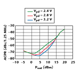
IS-95 uses a modulation scheme that requires a linear transmit path. With HBT technology, better linearity is achieved for less current. Adjacent-channel power rejection (ACPR) is a method of testing linearity under more realistic conditions. ACPR measurements for the RF2351 device were taken using IS-95 CDMA signals with an offset of 1.25 MHz. At +10 dBm output the ACPR was below -60 dBc with Vpd at 2.8 V. Figure 5 shows a plot of ACPR measured with different Vpd voltages.
Conclusion
The RF2351 PCS PA driver provides two selectable outputs to interface with split-band SAW filters and reduce the noise power in the receiver. The RFIC provides high gain, good noise figure and high linearity. It also allows some design flexibility. With outstanding performance, low cost and small size, the RF2351 helps to simplify RF system design. The ICs are manufactured on a four-inch GaAs HBT fab and are currently available for approximately $1 in production quantities.
RF Micro Devices Inc., Greensboro, NC (336) 664-1233.