
A Novel Surface-mount Approach to
Crossover Signals
Anaren Microwave Inc.
East Syracuse, NY
Because some locations require RF signals to cross RF, RF to cross DC, or DC and DC to cross each other, a significant number of multilayer PCBs are produced. Different approaches exist so that the additional layer can be avoided, but if good performance (that is, low insertion loss and high isolation) is desired, most designers will choose the multilayer solution.
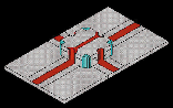
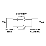 Balanced power amplifiers are one example of an application where crossing over signals is required. In this case, the DC bias line is required to cross over the RF lines. A basic balanced power amplifier block diagram is shown in Figure 1 . In this application, a designer can either run the DC signal under the DC blocking caps or run the DC signal on the backside of the board. No easy and inexpensive solutions exist today, but a more versatile and lower cost solution is being sought that will work for any combination of RF and DC crossover signals. This article briefly describes several signal crossing schemes and presents two surface-mount approaches that provide an easy solution for the designer as well as different design considerations for the components for RF and DC power handling.
Signal Crossing Schemes
When a designer is faced with a PCB design problem that cannot be solved without crossing two signals, a trade-off must be made in terms of cost (including manufacturability) and circuit board space. Of course, the electrical performance demands must be met for isolation, insertion loss, and DC current and/or RF power handling capability. Four different approaches are described as well as their pros and cons.
 Capacitively Coupled Lines
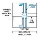
An approach that can be used for both RF crossing RF, DC crossing DC and even DC crossing RF is capacitively coupled lines, as shown in Figure 2 . Basically, the two lines crossing each other are printed on opposite layers and narrowed down at the crossing region to provide the desired amount of isolation. If high isolation is desired, the line(s) must be very narrow in order to limit the area of coupling. Narrower lines mean that the power capability for DC and RF is reduced and, of course, the insertion loss increases as the line width becomes narrower. When used with RF signals, a compensation for the discontinuity introduced must be made with shunt stubs that are located one-quarter wavelength away from the neck-down area on each side.
Another alternative utilizes series quarter-wave transformers going away from the neck-down area. This type of tuning is very band limited, and high isolation can be expected only in a very narrow bandwidth (though wide enough for most commercial applications). The advantage of this type of crossover is that it only requires printed circuitry and a couple of feedthrough holes and, therefore, is relatively inexpensive provided the board real estate is allocated. It is also important to consider how the PCB is attached to its cabinet. If mounted directly onto a heat sink, for example, the area underneath the backside circuit traces must be cleared by milling out cavities in the heat sink.
 Surface-mount Devices
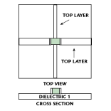
When building balanced power amplifiers as previously described, the problem of crossing RF and DC signals often is solved by running the DC lines underneath a large surface-mount technology (SMT) DC blocking capacitor, as shown in Figure 3 . The large cap typically is used to block the DC from the transistors to the RF input. However, it is necessary to use a large-sized chip to make the DC line wide enough to carry its required current, fit underneath the chip and not sacrifice isolation to the RF lines. When allowing for pick-and-place tolerances and isolation requirements, the line must be very narrow unless a very large (and, therefore, very expensive) capacitor is used.
The solution of crossing underneath an SMT device is feasible for DC crossing RF signals if line widths are narrow enough to provide sufficient isolation and DC current. For DC and DC, a similar approach uses SMT inductors or any other SMT component that is DC conducting. However, for RF crossing RF signals, the solution is not feasible in most cases because of limited isolation and the compensation that is required for the discontinuity introduced in the RF line underneath the capacitor.
 A Multiple-layer Design
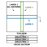
Using multiple layers, shown in Figure 4 , can yield a very high performance solution, but at an increased cost. Theoretically, the total number of copper layers needed is four (three physical board layers): the first layer for trace one, the second layer for the ground plane acting as the bottom of the top microstrip layer and as the isolator between traces, the third layer for trace two and the fourth layer for the last ground plane. The last ground plane layer (the third physical layer) can be eliminated if the multilayer board is mounted directly on a metal plate that acts as the ground plane. However, a cavity is required underneath the second layer’s circuit traces to make this scenario possible.
The ground layer between the two traces ensures good isolation and performance. Therefore, the lines can be kept as wide as desired for either the required RF impedance or the DC current capability. However, the solution is very expensive if used just for the sake of providing a crossover function.
Coaxial Cable
The oldest and simplest solution to crossing RF over RF signals is the use of a piece of coaxial cable. For DC over DC or DC over RF, a simple piece of wire can be used. The solution offers a designer great performance in terms of good isolation and low insertion loss. Major drawbacks of the solution are its limitations when considering high volume manufacturing. Phase consistency is a potential performance problem if it has to be repeated in volume due to the length of the cable and its solderability. However, no manufacturing engineer will approve the use of cables in a high volume design. For breadboard design and an occasional “oops” solution the approach can be used, but that is all that is recommended.
Crossover Component Design
It was found desirable to develop a surface-mount crossover component that creates a high performance solution -- a small, inexpensive and easy-to-use unit for breadboard and high volume design. Performance, size and cost must be compared to the other four described alternatives and should work for any combination of two RF and/or DC signals that must cross each other.
Component Size
Looking at the four described solutions, each can range in size from 0.1" x 0.1" (a large SMT cap) to larger than two times a quarter-wavelength. Even when considering, for example, the high frequency U-NII band at 5.5 GHz, the two quarter-wavelengths could be 2" x 0.02" given a high dielectric of 10. Remember that if two RF signals are crossing each other, two quarter-wave-long lines plus stubs are required in each direction; that is, in each path. Considering an application in the AMPS-band frequency range, the length of a quarter-wave is quite significant and the size of the capacitively coupled crossover circuits becomes much too large. Therefore, it is desirable to locate a component that is approximately the size of a large SMT capacitor and at least as small as 0.4 in2 .
Number of Layers
Theoretically, an SMT component adds a layer to the existing (two) PCB layers it will be mounted on, and it should be possible to construct a crossover component in two physical layers. The top layer of the SMT crossover with the circuit trace should act as a microstrip line with another dielectric layer underneath, as shown in Figure 5 . If this line is optimized for 50 W, the path can be used for RF or DC if the line width is wide enough for the required DC current. If the application requires RF over DC, the top layer can act as a bridge over the DC line and then can be left printed on the circuit board. The line width of the DC line must be small enough to fit underneath the crossover component and carry the desired DC current.
 However, the path that runs underneath will be a challenge to use for RF signals since the line’s width in the area underneath the crossover component now becomes a stripline. Although this development alone is not considered a major challenge, the components of the SMT crossover and the PCB may consist of different dielectric materials, creating a nonhomogenous medium there could even be air between the trace and component. In addition, a neck-down must be made, adding a discontinuity that must be compensated for.
To cross over RF and RF with the two-physical-layer crossover component, a number of design iterations can be expected or, if an appropriate electromagnetic simulator is used for a couple of hours, all of these issues can be compensated for. However, the scope of this component provides an easy-to-use solution. Therefore, a second part designed specifically for RF crossing RF will be developed so that the PCB designer will not have to deal with these issues. A three-physical-layer crossover component can be constructed where the top trace is left as a microstrip but the bottom trace is created in a stripline package, eliminating any effects caused by the PCB and the crossover component not being the same dielectric materials.
Terminal Locations
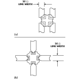
Another consideration for the surface-mount crossover components is to determine where the terminals for the traces should be located. Traditional Xinger® components have located the terminals in either the centers or the corners of the parts. The terminal itself is either a half-barrel (if located on the side of the part) or a quarter-barrel (if located in the corner of the part). This type of terminal, no matter where it is located, makes an easy-to-inspect solder joint when compared to a pad located only on the bottom of the part. However, the barrel creates a challenge for the designer because of the discontinuity it adds (by the vertical travel) and the pads on the top and bottom of the part. An easy-to-solder terminal was chosen since the electrical challenge can be solved and works well for even high power applications. The crossover component also has this type of barrel terminal. If the terminal is located in the corner of the part, it is easier to run different line widths into the part from the PCB because the part can be mounted on the corners of the lines and no neck-down is needed on the circuit runs. The two types of terminals are shown in Figure 6 .
 A number of different designs were simulated. As the parts became smaller, it became obvious that the terminals had to be located on the centers of the parts (not in the corners) since isolation was degraded by cross-coupling from corner to corner in that configuration and from the 50 W circuit traces being too close. Looking at different applications, it was also observed that most crossings are performed perpendicularly. Therefore, the inconvenience of potentially having to neck-down the circuit traces, compared to its straightforward layout, is considered minor.
RF and DC Power Handling
The last consideration is the DC current and RF power handling capability, which is a function of the materials used, the size of the part and the type of line width, which constitutes a 50 W input looking into the component. Remember that the line width of the circuit traces inside the part and on top of the component must be compensated significantly because of the terminals’ influence. The RF insertion loss is intended to be less than 0.1 dB, and it is assumed that most applications will be less than 5 A for DC currents. The highest current applications are assumed to be for RF crossing DC when used for balanced power amplifiers.
Final Components
Two components that provide either an RF crossing DC or RF crossing RF capability have been designed and simulated. For DC crossing DC either one can be used. Both parts use Rogers RO4350,® which is a UL-rated material that can be used in high power applications and offers good RF performance at a reasonable cost.
 RF-DC Component
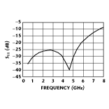
The RF crossing DC component is a two-layer part that is designed using two 20-mil RO4350 boards in a 0.2" x 0.2" package with the two terminals connecting the RF trace in the center of the two edges. All corners have terminals that connect the internal ground plane layer to the PCB’s ground. In order to compensate for the vertical travel in the half-barrel, the line width must be very inductive. In fact, the line width shrank from a typical 42-mil line width for a 50 W trace in a 20-mil-thick RO4350 material to approximately 24 mils. The compensation to the very narrow line width produced a good input return loss over a wide bandwidth. The power handling decreased but the insertion loss remained less than 0.1 dB as desired due to the very short line length. The input match is better than 25 dB up to 5.4 GHz, as shown in Figure 7 . The isolation depends on how close the DC line is to the RF pads on the bottom of the component, but it should be better than 35 dB.
Due to the terminals on the bottom side, the maximum line width that can be accommodated for the DC trace is approximately 95 mils, which is sufficient for more than 5 A in a 2 oz copper trace given reasonable ambient temperatures. In the current calculation, it is important to take into account whether the crossover is sitting directly on the DC run or if air is present between the part and the trace.
RF-RF Component
The RF crossing RF component is a three-layer part designed to use three 20-mil RO4350 boards in a 0.2" x 0.2" package. This part has four terminals connecting the RF traces; both sets of terminals are located in the center of the part. All corners also have terminals that connect the internal ground plane layer to the PCB’s ground. In order to compensate for the vertical half-barrel travel, which is now a little longer than the two-layer part (by more than 20 mils), the top circuit trace must be more inductive because less series inductance is present. The internal stripline trace is in a 40-mil ground plane spacing stack-up, which produces a compensated line width of only 9 mils.
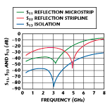 With both traces compensated, good performance is achieved over a wide bandwidth, as shown in Figure 8 . The insertion loss for both traces remains less than 0.1 dB as desired, due to the short length of the lines. The input match for microstrip exceeds 30 dB up to 4 GHz while a significant degradation occurs above that range. For the stripline, input return loss is greater than 20 dB to 6 GHz, and the isolation between the two traces is greater than 38 dB up to almost 6 GHz.
Conclusion
An inexpensive surface-mount crossover alternative that provides a crossover functionality with any desired combination of RF and DC crossing has been presented. One part was designed for RF crossing RF while the other was optimized for RF crossing DC. Any other combination can be performed using either of the two parts, depending on whether the objective is DC current capability or RF performance. Additional information may be obtained via e-mail at crossover@anaren.com.
Anaren Microwave Inc., East Syracuse, NY (800) 544-2414.