
Fifth generation wireless access networks are expected to meet system and service requirements of new use cases and applications in 2020 and beyond. 5G new radio (NR) envisages providing 10 Gbps peak data rates per user, roughly 100x improvement over the fourth generation wireless access network. 4G LTE-Advanced Pro, also termed by some vendors as 4.5 to 4.9G, can achieve up to 1 Gbps peak data rates using wider bandwidths and carrier aggregation. Sustained data rate per user in LTE-Advanced Pro typically ranges between 25 to 50 Mbps. 5G NR targets 100x improvement by pushing sustained data rate per user to 500 Mbps.
Significant increase in spectral efficiency and tapping into underutilized spectrum above 6 GHz are key enablers of multi-gigabit data rates for enhanced mobile broadband (eMBB). Massive MIMO, or large arrays of antennas, is the keystone technology for realizing this improvement. Massive MIMO adds spatial dimension in addition to frequency and time to significantly boost spectral efficiency. The resulting signal-to-noise ratio (SNR) improvements brought about by the array gain and orthogonality of multiple beams means the same time and frequency allocations can be used by multiple users.
Time-division duplexing (TDD) bands with wider bandwidths, such as band 41 (2496 to 2690 MHz) and band 42 (3400 to 3600 MHz), are the prime candidates for massive MIMO deployments below 6 GHz bands. Tapping into underutilized centimeter and millimeter wave bands, with large swaths of available bandwidth in frequencies such as 15, 28, 39 and 70 to 80 GHz, are critical components of 5G NR massive MIMO deployments above 6 GHz.
Total transmitted power by the full antenna array could typically range from 40 to 100 W, but power per antenna based on the number of antennas used in the array drops down to few hundreds of milliwatts. This allows use of low cost and lower precision analog components in the final stages of a typical RF line up. Instead of using active signal chains per antenna with fully digital beamforming, hybrid schemes are proposed, where a single active signal chain is shared by a set of antennas, with beamforming functionality performed partly in the digital domain and partly in the analog domain using phase shifters.
The power, footprint and cost associated with deploying very high channel counts along with wider signal bandwidths are significant hurdles. Increased integration along with significant power reduction is required for commercial deployments. Integrating RF-class or RF sampling data converters into radio digital front-end system on chip (SoC) overcomes this hurdle by lowering power, footprint and cost of the total system.
Implementing a Viable 5G NR with RF SoC
A 5G NR massive MIMO implementation requires a large number of active signal chains in the radio to connect to each antenna or a subset of antennas in the array. These active signal chains are traditionally comprised of data converters, filters, mixers and power amplifier or low noise amplifier, and can lead to significant increase in power, form factor and cost of the system. The large number of active signal chains in massive MIMO systems—for digital or hybrid beamforming—makes system power and footprint too high to realize commercially viable systems. The costs associated with moving data between the RF front-ends (RFFE) and the digital front-end (DFE) is one of the key challenges that must be resolved in 5G—at the software, hardware and system level.
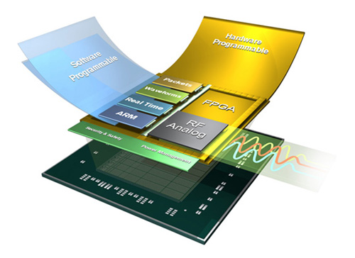
A newly introduced SoC technology tackles this through device integration. The platform, based on a 16 nm FinFET silicon process, monolithically integrates RF-class analog technology into a multi-processor SoC (MPSoC) for a fully hardware and software programmable radio frequency system on a chip, or RFSoC. Based on an ARM-class processing subsystem merged with FPGA programmable logic, the architecture features 12-bit, 4 GSPS RF sampling analog to digital converters (ADC), and 14-bit, 6.4 GSPS direct RF digital to analog converters (DAC), along with optimized digital down-conversion and up-conversion signal processing.
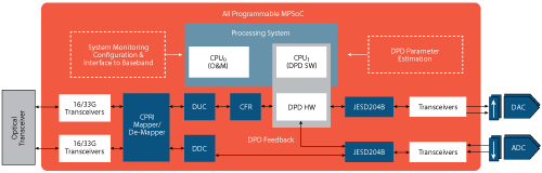
Figure 1 All programmable MPSoC as a DFE platform.
The RFSoC is built on an all programmable MPSoC architecture, an established platform for radio DFE implementations. As shown in Figure 1, the base architecture can employ the ARM processing subsystem for O&M functionality, digital predistortion (DPD) and protocol software, while the FPGA fabric can be utilized for high performance data path functionality, control logic and high speed interfacing. Now with the integration of communication-grade RF sampling ADCs and DACs and the removal of multiple discrete components, RFSoCs enable compact radio form factor with potential for embedding DFE functionality within or behind antenna arrays. The result is new levels of power efficiency, form factor reduction, shortened design cycles and design flexibility urgently needed for LTE-Advanced Pro, 5G active antenna systems and massive MIMO radios.
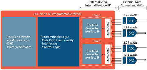
Figure 2 Radio DFE interfacing to external wideband data converters.
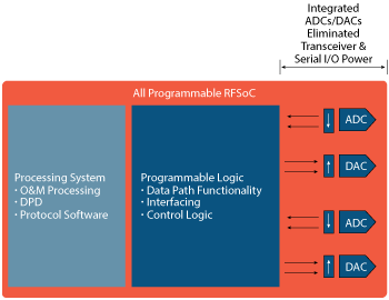
Figure 3 Elimination of RF component power and interface power.
Power Reduction
Figure 2 illustrates the high-power cost of moving data from a wideband (1 GHz) 2 × 2 RFFE into the DFE for processing using discrete RF sampling data converters. Even with integrated digital down-conversion (DDC) or digital up-conversion (DUC) in the data converters, large amounts of data still need to be sent to and from the DFE. The I/O power number shown for each quad transceiver (1 W per four lanes) includes the power associated with implementing JESD204B Protocol—on 16 nm MPSoC devices. In addition to interface power, the power consumption of the discrete data converter components remains high. A typical single channel RF sampling ADC may consume ~2.25 W, and an RF sampling DAC ~1.75 W.
DFE signal processing, as shown in Figure 1, has leveraged the latest deep-submicron CMOS technologies to reduce power, while RF and other analog components have traditionally leveraged older-process technology. The older CMOS and even BiCMOS technology offered the required performance at the right costs for these predominately analog (“Big A”) discrete components. However, the move to a more digitally dominated SoC (“Big D”) means that it is now commercially viable to build data converters on the latest advanced CMOS technologies, allowing huge power and cost savings. Integration of these data converters is represented in Figure 3.
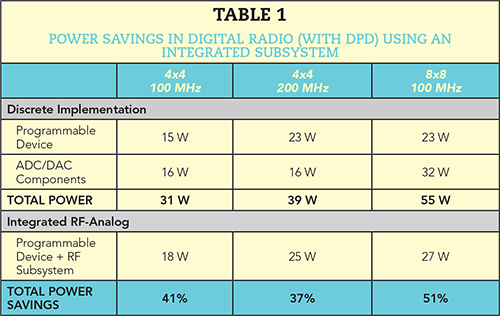
On the SoC device itself, the integration of the data converters eliminates the need for the JESD204B IP cores and use of the device’s high speed serial transceivers. With the elimination of components, interfacing, IP and use of transceivers—as channel count increases so does system power reduction. Based on single channel RF data converters, elimination of all these factors results in 40 percent power reduction in a 4 Tx/4 Rx radio and over 50 percent power reduction for an 8 Tx/8 Rx system, as shown in Table 1.
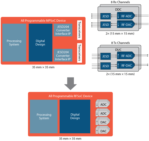
Figure 4 PCB area savings in 8 Tx/ 8 Rx radio.
System Form Factor Reduction
Radio form factor (size or volume) is a critical attribute for securing deployment in terms of rental fees, wind loading and compliance to the local government’s regulations and restrictions. Reducing radio unit volume is an important system design criteria. Integrating RF-class data converters results in significant saving, as shown in Figure 4. Form factor reductions are proportional to the number of antennas in the system. PCB area savings can range from 40 percent and reach 75 percent. An example of an 8 Tx/8 Rx radio using quad channel ADC and DAC are shown in Figure 4.
Shortened Design Cycles and Eliminating JESD204 Interface
Beyond power and form factor benefits, elimination of discrete data converters shortens the design cycle in several ways. Because most modern converters currently use high speed serial interfaces from 12.5 to 25 Gbps based on the JESD204 protocol, design closure is impacted at the digital, analog and system level. The JESD204 IP cores must be implemented in digital FPGA fabric, but arguably the more difficult task is ensuring a stable serial data link between the data converter and the radio’s DFE. At 12.5 Gbps and up to 25 Gbps, signal distortion is a serious concern mostly due to running high line rates over low cost, lossy interconnect. Eliminating the DFE and RFFE interface removes this burden and reduces the number of board layers, complexity of routing the clocks on the PCB and synchronization of the communication links.
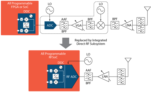
Figure 5 Comparison of superheterodyne and direct sampling receivers.
Design Flexibility with RF Sampling on 16 nm FinFET
Direct RF sampling DACs and RF sampling ADCs in the RFSoC eliminate the need for intermediate frequency (IF) stage sampling for 5G Radios implemented in sub-6 GHz frequency bands, thereby reducing the complexity of the RFFE, as shown in Figure 5. Direct RF sampling, integrated with highly optimized RF digital signal processing engines (i.e., DDC and DUC) offers a much more flexible approach to traditional analog frequency translation and filtering. The higher sample rates simplify the analog filtering requirements and allow a better trade-off between dynamic range (SNR) and signal bandwidth in the digital domain by decimating and filtering the ADC output to extract only the signal bandwidth of interest.1 Implementing the signal conditioning in the digital domain also yields better performance and ease of use. Some of the traditional RF impairments in the IF approach are greatly reduced or eliminated (e.g., passband ripple, group delay variation, matching and local oscillator (LO) leakage issues).
With advanced CMOS technology, namely 16 nm FinFET, RF signal processing can be implemented in the digital domain with excellent power and cost efficiency. At 16 nm, the RF sampling solution in the RFSoC architecture delivers a flexible RF front-end while supporting wide bandwidths—up to 2 GHz—at a much lower power draw than required by analog technologies.
Demonstrating ADC and DAC Performance
New digitally assisted techniques allowed designers to address the challenge of integrating state-of-the-art RF sampling converters using advanced CMOS technology.2 By using very cost and power efficient 16 nm FinFET digital transistors, it is possible to add very sophisticated digital calibration to correct for any analog circuits impairments. This approach to implementing advanced RF sampling converters delivers large benefits in terms of power and area reduction. It also provides a platform technology that will scale with Moore’s Law to 7 nm and beyond.
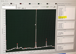
Figure 6 RF DAC generating two tones at 1.9 GHz separated by 20 MHz.
Results from a 16 nm FinFET test chip featuring the RFSoC’s direct RF sampling converters show excellent performance, linearity and analog characteristics of a 6.8 GSPS RF DAC and 4 GSPS RF ADC—evaluated across process, temperature and power supply variation.2 The built-in calibration and digitally assisted techniques deliver very consistent and stable performance across PVT.
The output of the DAC generates two tones at a carrier frequency of approximately 1.9 GHz separated by 20 MHz, as shown in the output of the Rohde & Schwarz FSW Spectrum Analyzer in Figure 6. The 3rd order intermodulation illustrates the very high linearity of the DAC at approximately -75 dBc. This is within the first Nyquist zone, which extends up to 3.2 GHz. The 2nd and 3rd order images folded back also show excellent performance of the DAC.
For the ADC, a high quality signal sourced by the Rohde & Schwarz SMW200A vector signal generator is used to synthesize both CW and modulated waveforms. Additional analog filtering by the signal source provides the signal purity required to evaluate the ADC. The captured data is analyzed using fast Fourier transforms (FFT) implemented with LabView Software from National Instruments, as shown in Figure 7. The FFT of a -3 dBFS 1.9 GHz CW signal is sampled at 4 GSPS, and the plot shows the first Nyquist zone of the ADC. The 2nd and 3rd order distortion components are aliased into the first Nyquist zone as indicated by the red markers. Other distortion components shown are interleaving artifacts which are greatly suppressed using built-in calibration.
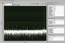
Figure 7 FFT of a continuous wave tone sampled at 4 GS/s by the RF ADC.
Meeting the Design Challenges and Application Constraints for RFSoC
As with any complex SoC, there were tradeoffs and design choices made when developing the all programmable RFSoC. This ranged from meeting challenging power targets, to careful consideration of the constraints hardware designers face when realizing their end application, to providing a platform with the correct mix of optimized and programmable signal processing.
Power Density
With reduced form factor and significantly greater performance, 5G NRs face tough power density challenges and present a thermal engineering problem. The system is typically passively cooled with high operating ambient temperatures generated by the power amplifier and other components. In order for components to stay within their specified operating temperature range, they typically cannot dissipate more than 35 W before the thermal solution becomes complex and costly.
While integrating RF sampling data converters greatly reduces the system power, it must also not significantly increase the power dissipation of the SoC. Ideally, the solution would be power neutral with the converter power being similar to the power dissipated by the external IO interfaces like JESD204B. This drove many of the design choices and techniques used in developing the RFSoC, including digitally assisted analog and interleaving to reduce the power consumption of the converters.
Practical Hardware Solutions
The RFSoC needed to meet key requirements like channel to channel RF isolation (which typically needs to be greater than 70 dB) and immunity to other sources of noise in what is a highly mixed signal environment. The SoC is a predominately digital (Big “D”) device that supports external memory interfaces, along with system interfaces like 100GE and common public radio interface (CPRI). Through careful design and floor planning of the SoC, along with package and PCB co-design, RFSoCs can achieve very robust performance without costly PCB design rules or nonstandard manufacturing techniques.
Maximizing Flexibility
Traditional SoC implementation involves tradeoffs in functionality, cost and power consumption. Developing the RFSoC was no exception but benefited from significantly more degrees of freedom. Generic functionality like DDC was implemented in highly power efficient 16 nm FinFET logic; however, much of the application specific functionality can be efficiently implemented in the programmable logic. The RFSoC achieves a balance between dedicated hardened digital signal processing and user configurable high performance processing. The result is an all programmable platform for implementing a range of applications beyond just radio.
The choice of advanced CMOS technology like 16 nm FinFET is a key part of maintaining this flexibility to adapt to changing standards and allow designers to react quickly to emerging requirements. The direct RF sampling moves the RF into the digital signal processing domain as soon as possible, where it can be processed very efficiently in the digital domain using advanced CMOS technology.
Aligned with 3GPP Specification Timelines
The introduction of all programmable RFSoCs is well aligned with 5G NR specification timelines. The draft of the 5G NR non-standalone specification (release 15) is targeted to be available by December 2017. The Standalone 5G NR portion of the release 15 specification is expected to be completed by June 2018. Non-standalone mode will use LTE as the control plane anchor. 5G NR control plane for standalone mode will be defined in the June 2018 release. The 3GPP industry workgroup is debating on the extent of the ultra-reliable low latency communication (URLLC) use case to be covered in release 15. Due to tight timelines for release 15, many facets of the URLLC use case are targeted in the 5G NR release 16 specification scheduled to be available by end of calendar year 2019.
Summary
With all programmable RFSoCs, the ability to leverage the same hardware to address diverse requirements and emerging standards will allow vendors to quickly react to new market opportunities by leveraging existing developments. In the case of 5G systems it is becoming clear that no one type of radio will address the diverse needs of next generation radio access networks (RAN) and so the number of different radio types is expected to increase significantly.3
References
- Boris Murmann, IEEE Micro, Volume: 26, Issue: 2, March-April 2006: “Digitally Assisted Analog Circuits.”
- While the test chip demonstrates a 6.8 GSPS DAC, All Programmable RFSoC specifications currently target 6.4 GSPS DAC performance.
- “Final report on the METIS 5G System Concept and Technology Roadmap,” METIS Deliverable D6.6, https://www.metis2020.com/wp-content/uploads/deliverables/METIS_D6.6_v1.pdf