
K-band Quadrature Mixers with Plastic-packaged Diodes
Matjaz Vidmar
University of Ljubljana, Slovenia
Quadrature mixers (also known as IQ mixers) are important signal-processing components in radio transmitters (as vector modulators) and radio receivers (as image-reject mixers and/or demodulators) as well as other microwave equipment (phase-locked loops (PLL)). A quadrature mixer requires two balanced mixers that are precisely matched in amplitude and operated at an accurate 90° phase shift. Precise amplitude matching and exact phase shifts are increasingly more difficult to obtain at higher frequencies. At K-band frequencies, the best technical solution is probably monolithic integration.1,2 However, there are other possible hardware implementations that should not be neglected.
In this article, two practical K-band, quadrature mixer designs are presented using inexpensive, packaged semiconductor devices installed on conventional printed circuit boards. Although most packaged semiconductor devices were developed for operation at relatively low frequencies (usually below 3 GHz for the mass mobile phone market), the mixer's small package size and excellent chip characteristics allow useful performance even in the K-band frequency range. The first application example is a 20 Gbps clock recovery circuit that requires a quadrature phase detector in its PLL. The second application is a direct-conversion (zero IF) 24 GHz industrial, scientific and medical (ISM) band radio transceiver that requires quadrature mixers both in the transmitter modulator and the receiver demodulator. Finally, a practical test method for quadrature mixers is presented that allows quick and efficient circuit optimization as well as verification of all important quadrature mixer parameters.
 The Antiparallel Diode Mixer
At K-band and higher frequencies, the antiparallel diode mixer is a popular solution since it requires a subharmonic LO at one-half the conversion frequency. (In other words, the antiparallel diode mixer has a built-in LO frequency doubler.) On the other hand, the antiparallel mixer 's insertion loss and noise figure as well as the intermodulation distortion (IMD) are worse than those of fundamental LO mixers, and the antiparallel mixer is much more sensitive to the LO signal level than fundamental LO mixers.
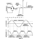
The principle of operation of an antiparallel mixer is shown in Figure 1 . The I/V curve of a perfect antiparallel diode pair is an odd functon that can be represented with a polynomial with just odd powers of V (C1, C3, C5, C7, ...). One of the third-order conversion products, the RF input minus twice the LO, is the desired conversion product of a mixer with a subharmonic LO. Of course, other third- and higher-order conversion products cause IMD.
In an antiparallel mixer, the highest conversion efficiency is obtained when each diode conducts for approximately 90 electrical degrees of the LO signal. When the LO level is too low, the conversion efficiency may drop to zero if the diodes are not turned on at all. On the other hand, when the LO signal level is too high, either one or the other diode is turned on most of the time, again resulting in little impedance change and poor conversion efficiency. Conventional silicon Schottky diodes typically require an LO level between 0 and 10 dBm for the best conversion efficiency in an antiparallel mixer in a 50 W environment.
 A frequently forgotten, but important, attribute of the antiparallel mixer is that it is a balanced mixer. Thanks to the odd transfer function of a perfect antiparallel diode pair, rectification and second-harmonic generation are not possible. Even more important at very high frequencies, the mixer balancing of an antiparallel mixer is obtained without critical and complex baluns. Good mixer balancing is important in a phase detector to reduce the output offset voltage. Good mixer balancing is also important in a receiving mixer to suppress LO noise, especially at very low intermediate frequencies or in direct-conversion receivers. Finally, good mixer balancing is also required in a vector modulator in a transmitter to suppress the residual carrier.
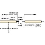
Since the RF, LO and IF frequencies are widely separated and no balun is required, antiparallel mixer circuits are usually simple. At low IF values, the RF is close to the second harmonic of the LO frequency. Therefore, the conventional antiparallel mixer circuit, shown in Figure 2 , includes just an open stub and a shorted stub. Both stubs are one-quarter wavelength at the LO frequency and one-half wavelength at the RF. The IF is coupled through a simple LC lowpass.
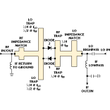 Unless two monolithically integrated diodes are used as the antiparallel pair, package and circuit parasitics may corrupt the mixer balancing. When using single-packaged diodes at K-band frequencies, a completely symmetrical circuit is required for good mixer balancing, as shown in Figure 3 . An additional advantage of the symmetrical circuit is that no critical connection to ground (vias in the microstrip board) is required. The IF can be taken either from the LO or RF side of the mixer. In both cases, an IF return to ground must be provided on the other side of the mixer. The quarter-wavelength RF traps introduce a substantial mismatch for the LO signal so additional LO matching stubs are always required. Little if any matching is required on the RF side of the mixer since the quarter-wavelength LO traps behave as half-wavelength resonators at the input RF.
BAT14-02W single silicon Schottky diodes, manufactured by Infineon Technologies (formerly Siemens Semiconductors), are used in the described K-band antiparallel mixer. This medium-barrier diode (430 mV forward drop at 1 mA) is packaged in the very small SCD80 plastic surface-mount device (SMD) package. An antiparallel mixer with two BAT14-02W diodes requires approximately 7 dBm of LO power for operation at K-band frequencies.
A 20 Gbps RZ Clock Recovery Application
In optical-fiber communications, specially shaped lightwave pulses called solitons are frequently used for data rates beyond 10 Gbps. In the receiving photodiode the soliton pulses are converted in a return-to-zero (RZ) electrical data stream. RZ-encoded data have a very strong, discrete spectral line at the clock frequency. An RZ clock recovery can be simply a narrow bandpass filter (BPF) tuned to the clock frequency.
A PLL is frequently used as a narrowband filter in clock recovery circuits. A suitable second-order feedback network in the PLL can remove any static clock phase errors regardless of component tolerances and clock frequency offset. Unfortunately, the inital frequency offset of such a PLL may be much larger than the acquisition bandwidth of the PLL. A search logic function together with a reliable lock detector are therefore required in a PLL-based clock recovery circuit. A clock recovery PLL requires two phase detectors operating in quadrature. The in-phase (I) detector provides the lock information while the quadrature (Q) detector provides the loop feedback. In the unlocked state, the search logic scans the entire frequency range of the VCO. As soon as lock is detected, the feedback loop is closed by connecting the Q detector output to the VCO control input.
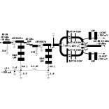 The circuit diagram of a practical 20 GHz quadrature phase detector is shown in Figure 4 . The circuit includes a two-stage, selective RF preamplifier and two antiparallel mixers with BAT14-02W diodes. Both mixers are fed in phase with the 10 GHz LO signal. A 90° phase shift is introduced by the RF input line to the Q mixer because it is one-quarter wavelength longer than the corresponding line to the I mixer. Both RF and LO signals are split with Wilkinson dividers to reduce the crosstalk between the two mixers.
The selective RF preamplifier has a gain of approximately 13 dB, including the 20 GHz BPF 's insertion loss. The BPF is required to prevent overloading of both mixers with the wideband signal coming from the photodiode. An RF input of -10 dBm at 20 GHz produces I and Q outputs of approximately ±150 mV across a high impedance load with a nominal +10 dBm LO drive at 10 GHz.
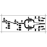
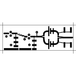 The 20 GHz quadrature phase detector is built as a microstrip circuit etched on 0.5-mm-thick (19 mil) Rogers Corp. Ultralam 2000 laminate with a dielectric constant of 2.43. Since the circuit is a prototype, there are no plated-through holes. All components are grounded through 3.2 mm (1/8") diameter holes in the laminate that is covered with 0.1-mm-thick copper foil on the ground plane side. The 80 x 30 mm circuit pattern is shown in Figure 5 .
Each of the 1 pF capacitors is made with two 0.5 pF, 0402-size ceramic capacitors installed in parallel to minimize the discontinuities on the microstrip lines. All resistors are 0805 size. The resistors in the RF part of the circuit (the two 330 W resistors in the gates of the FETs and the two 100 W resistors in the Wilkinson dividers) are installed upside down with the resistive layer facing the surface of the printed circuit board.
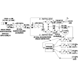 The block diagram of the 20 Gbps RZ (soliton) clock recovery is shown in Figure 6 . The clock recovery includes a high speed photodiode, an additional 20 GHz narrowband amplifier, a 20 GHz quadrature phase detector, a PLL search logic function, a PLL loop amplifier and a 2.5 GHz VCO followed by phase shifters and frequency multipliers. The EPITAXX EPM820FJ-S high speed photodiode includes an internal 50 W termination and is specified for 15 GHz bandwidth operation. The expected optical input sensitivity is approximately -5 dBm. Depending on the shape of the input (soliton) optical pulses, even better sensitivities were observed in practice. Due to the large impedance mismatch between the high impedance photodiode and the 50 W system, a -5 dBm optical input only produces an RF signal of approximately -35 dBm at 20 GHz, therefore, an additional amplifier is required in front of the phase detector.
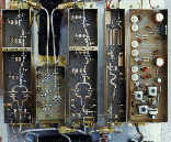
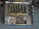 The remaining circuits of the 20 Gbps clock recovery are designed around the same phase shifters and other circuits described previously.3 The VCO is operated at 2.5 GHz to allow simpler phase shifters followed by frequency multipliers. The 20 Gbps clock recovery circuit supplies two main 10 GHz clock outputs for the 20/10 Gbps demultiplexer (D-flip-flop) and the 10 Gbps error detector. Both 10 GHz clock outputs have independent phase shifters. An additional 2.5 GHz output is provided as a trigger for a sampling oscilloscope. Finally, an additional phase shifter is built in the PLL itself, supplying the 10 GHz LO to the 20 GHz quadrature phase detector. This additional phase shifter is very convenient when the optical-fiber length in front of the clock recovery is changed while all other optical and microwave connections remain unchanged. The described clock recovery design was intended for particular laboratory experiments that required different output options. Although a direct 20 GHz output could be easily implemented, it was not provided since it was not required for the aforementioned experiments. Figure 7 shows the completed clock recovery assembly.
A 24 GHz Direct-conversion Transceiver
Direct-conversion transceivers include a direct vector modulator in the transmitter and downconversion to a very low IF in the same range as the baseband modulation signal in the receiver. Critical and expensive microwave hardware (such as narrow BPFs) is not required since there are no image responses or other close-in spurious signals to be filtered out. A direct-conversion or zero-IF transceiver is, therefore, a promising solution for no-tune, low cost, mass-market applications if simple and reliable quadrature mixers are available for the frequency range of interest.
In direct-conversion or zero-IF transceivers, the subharmonic-LO mixer has yet another advantage. Since the subharmonic LO operates on a different frequency from the RF front end of the transceiver, much less shielding is required to prevent LO leakage from being picked up by the receiving antenna. Less shielding is also required to prevent the transmitted signal from disturbing the LO source. Poor LO shielding, resulting in an interaction with the RF front end of the transceiver, corrupts the balance and quadrature offset of both receiving and transmitting mixers. The quadrature errors are usually a major drawback of direct-conversion designs.
To check the feasibility of direct-conversion designs, a Weaver single-sideband (SSB) analog voice transceiver for 24 GHz was designed, built and tested. The transceiver includes quadrature mixers with antiparallel diodes both in the transmitter and the receiver. Of course, a similar transceiver design also could be used for biphase or quadrature phase-shift keying data transmission in the 24 GHz ISM band.
 The design of the 24 GHz quadrature receiving mixer, shown in Figure 8 , is very similar to the already described 20 GHz phase detector. Two simple 12 GHz BPFs are added to prevent low frequency noise from the LO from disturbing the weak I and Q IF signals. Two IF preamplifiers with two Philips BF199 transistors are included in the quadrature mixer module for a similar reason. Both IF preamplifiers receive their supply voltage from the following quadrature IF amplifier.
The 24 GHz RF preamplifier is also similar to the 20 GHz version. Unfortunately, the ATF35076 pseudomorphic high electron mobility transistors are only specified up to 18 GHz by their manufacturer.4 While it is relatively easy to match these devices at 20 GHz, it is much more difficult to obtain useful gain from them at 24 GHz, probably due to an internal package resonance. Tuning stubs at both input and output are required to obtain a gain similar to the 20 GHz version. Both transistors operate at a zero gate bias for maximum gain. The gate bias network includes a lowpass filter and a 68 W resistor to decrease the gain at lower frequencies. Red light-emitting diodes (LED) are used as very low noise shunt regulators for the drain supplies of both transistors. Supply regulators are required since the 24 GHz transceiver supply is +12 V.
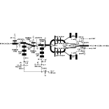
 The 24 GHz quadrature receiving mixer is built as a microstrip circuit etched on 0.5-mm-thick (19 mil) Ultralam 2000 laminate with a dielectric constant of 2.43. The circuit pattern is shown in Figure 9 and has dimensions similar to the 20 GHz phase detector (80 x 30 mm). The only difference in the construction from the 20 GHz phase detector is two 1 nF feedthrough capacitors installed in 3.2-mm-diameter (1/8") holes in the substrate. The tuning stubs are small pieces of 0.1-mm-thick, pretinned copper foil.
The noise figure of the described 24 GHz quadrature mixer is high. Experiments have shown that most noise comes from the 12 GHz LO, especially with a very low IF as in the case of a Weaver SSB voice receiver. In addition to the built-in, two-stage preamplifier, a low noise amplifier gain of at least 25 dB is required to mask the LO noise.
The 24 GHz quadrature transmitting mixer (vector modulator) is identical to the receiving mixer. The 12 GHz LO signal level is increased to approximately 14 dBm to obtain a higher output power at 24 GHz. At higher LO levels, the BAT14-02W diodes generate high order harmonics in the millimeter-wave region. High order harmonics corrupt the mixer balancing and may even cause interaction between the two antiparallel mixers. A very simple countermeasure for this interaction may be to swap the two mixer diodes of one antiparallel mixer to flip the phase of the offending harmonic.
 The transmitting mixer includes a two-stage selective RF amplifier at 24 GHz. This amplifier is identical to the RF preamplifier in the receiving mixer except that the input and output are swapped. An undistorted SSB signal of approximately -3 dBm at 24 GHz is obtained at the output of the two-stage RF amplifier. Of course, the complete transceiver, shown in Figure 10 , includes additional amplifier stages to increase the transmitter output power as well as improve the receiver noise figure.
 Testing Quadrature Mixers
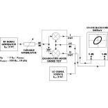
The specification of a quadrature mixer requires several parameters to be tested. Besides the parameters of the single mixers, precise 90° phase offset and gain tracking between the two mixers also are required. A simple and quick test procedure to display all important quadrature mixer parameters is required for tuning or optimizing a circuit during development. The suggested mixer test setup, shown in Figure 11 , can be used to characterize phase detectors or receiving mixers with a very low IF. Very low IFs, comparable to the baseband modulation signals, are used in direct-conversion transceivers. The same setup can also provide useful data for transmitting mixers since most interesting mixer parameters are reciprocal under small RF/IF signal conditions.
While working with mixers, a suitable LO source is usually available as part of the equipment where the mixer is going to be used. A CW signal generator equipped with a variable attenuator is also a standard piece of test equipment for testing receivers. The only additional item required is a low frequency XY oscilloscope display. The bandwidth of the oscilloscope should include the expected IF range (usually less than 1 MHz in direct-conversion transceivers).
The RF signal generator is tuned to a frequency that has a small offset from the appropriate LO harmonic, depending on the type of mixer. The XY oscilloscope display then shows a rotating bright spot. The direction of rotation (clockwise or counterclockwise) depends on whether the RF signal generator is tuned below or above the appropriate LO harmonic.
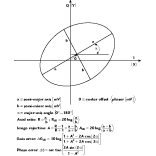 While making measurements on K-band mixers, a frequency offset between 100 Hz and 10 kHz is usually a practical choice. If the frequency offset is too low, the phase noise of both RF and LO signal sources makes the oscilloscope trace very noisy. If the frequency offset is too high, the frequency response of the IF network and XY display may corrupt the result. In all cases it is useful to check the XY display across the expected frequency range before making any actual measurements. A perfect quadrature mixer should display a perfect circle centered on the XY screen. Real quadrature mixers display an ellipse due to gain differences between the I and Q channels and a phase offset different from the ideal 90°. Finally, the center of the ellipse is offset from the center of the XY display due to poor mixer balance, as shown in Figure 12 .
Antiparallel mixers with medium-barrier Schottky diodes such as the BAT14-02W types typically provide a linear output range of approximately ±150 mV across a high impedance load. If the RF signal level is further increased, mixer saturation occurs. The ellipse on the XY display becomes distorted. The first visible effect is usually an egg-shaped curve due to slight limiting in the mixer.
Poor quadrature mixer balance can be described with the ellipse-center offset phasor o. Poor antiparallel-mixer balance is caused by single-diode tolerances as well as high order harmonics at high LO drive levels. At an LO drive level of 10 dBm for the entire quadrature mixer (7 dBm per antiparallel mixer), the unbalance phasor magnitude was in the 15 mV range. In the transmit mixer, a residual carrier suppression of approximately -20 dB was measured at 14 dBm LO drive in a different test setup, confirming that reciprocity works in this case.
The mixer balance could be improved by selecting matched pairs of the BAT14-02W mixer diodes. It should be noted that the BAT14-02W diodes used in the experiments were the very first preproduction samples obtained from the manufacturer. Fine-tuning of the mixer balance can be adjusted by precise positioning of the diodes on the printed circuit board. Since the diodes are soldered to the printed circuit board as conventional SMD components, they can be repositioned by simple soldering operations.
The most important parameter of a quadrature mixer is probably the axial ratio R of the ellipse observed on the XY oscilloscope display. The axial ratio defines the image (or unwanted-sideband) rejection A of a quadrature mixer. If the inclination angle a of the major axis of the ellipse is also known, the exact cause of the ellipticity can be determined (gain error, phase error or both). This information is very useful when developing or tuning the quadrature mixer circuit. A major-axis angle close to 45° or 135° indicates that the phase offset between the I and Q mixers differs from the ideal 90°. A major-axis angle close to 0° or 90° indicates a gain difference between the I and Q channels. Most importantly, the effects of additional tuning stubs can be observed immediately on the XY oscilloscope display.
The designs of both K-band quadrature mixers presented in this article were optimized in the described test procedure. The final designs achieved an axial ratio of approximately 1 dB, corresponding to an image (or unwanted-sideband) rejection of approximately -25 dB. Due to the relatively thick microstrip board (0.5-mm Teflon at K-band), the unwanted effects due to microstrip radiation and reflections from the walls of the shielding enclosure were in the same order of magnitude.
Conclusion
Two practical K-band quadrature mixers were presented as part of a 20 Gbps clock recovery circuit or as components of a 24 GHz direct-conversion radio transceiver. Both designs use inexpensive, plastic-packaged SMD diodes soft soldered on inexpensive softboard substrates. The single mixers use antiparallel diodes to achieve subharmonic LO operation, good mixer balancing and good residual carrier suppression. A simple and efficient method for testing quadrature mixers also was presented. The described K-band IQ mixers achieve an image (or unwanted-sideband) suppression of approximately -25 dB without additional tuning.
References
1. Ali E. Ashtiani, Tacar Gokdemir, Georgios Passiopoulos, Ali Rezazadeh, Suengil Nam and Ian Robertson, "Miniaturized Low Cost 30 GHz Monolithic Balanced BPSK and Vector Modulators: Part I, " Microwave Journal , Vol. 42, No. 3, March 1999, pp. 100-108.
2. Ali E. Ashtiani, Tacar Gokdemir, Georgios Passiopoulos, Ali Rezazadeh, Suengil Nam and Ian Robertson, "Miniaturized Low Cost 30 GHz Monolithic Balanced BPSK and Vector Modulators: Part II, " Microwave Journal , Vol. 42, No. 4, April 1999, pp. 104-114.
3. Matjaz Vidmar, "Microstrip Resonant Phase Shifters, " Microwave Journal , Vol. 42, No. 9, September 1999, pp. 127-136.
4. Hewlett-Packard, Communications Components Designer's Catalog: GaAs and Silicon Products , 1993, pp. 7.73-7.75.
Matjaz Vidmar received his BSEE and MSEE from the University of Ljubljana, Slovenia in 1980 and 1983, respectively. He received his PhD in 1992, also from the University of Ljubljana, for developing a single-frequency GPS ionospheric correction receiver. Vidmar is currently teaching undergraduate and postgraduate courses in electrical engineering at the University of Ljubljana. His current research interests include high speed electronics for optical fiber communications. Vidmar is also taking part in amateur satellite projects. He developed very high efficiency VHF and UHF transmitters that were successfully flown in space on the Microsat mission in 1990.