
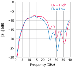
Figure 1 Input return loss vs. frequency.
A very wideband RMS power detector from Linear Technology resolves many of the challenges in achieving accurate power measurement of complex modulated signals at microwave frequencies. The LTC5596 RMS power detector offers:
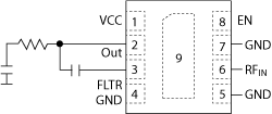
Figure 2 LTC5596 pinout and interface connections.
- A wide input frequency range from 100 MHz to 40 GHz and a very flat response, typically less than ±1 dB between 200 MHz and 30 GHz.
- 50 Ω impedance, without any external matching components (see Figure 1).
- 35 dB linear-in-dB dynamic range, with ±1 dB accuracy over the industrial (I) case temperature range from ‐40° to +105°C. The high temperature limit can be extended to +125°C with the H-grade version.
- High output, capable of driving 50 Ω loads.
- High insensitivity to large peak-to-average power ratios (PAPR), enabling accurate measurement of complex waveforms without extensive calibration.
- ESD ratings of 3.5 kV human-body model (HBM) and 1.5 kV charged-device model (CDM), easing handling in manufacturing environments.
By their nature, root mean square (RMS) power detectors are well-suited to accurately measure the average power of arbitrary waveforms. This is because such devices precisely implement the definition formula for average power, i.e., proportional to the average of the squared signal. Other types of power detectors, such as Schottky diode detectors or demodulating logarithmic amplifiers, implement slightly different operation that often involve the signal envelope. Their response changes whenever the input waveform—but not the average power level—is changed. Modern communication systems use complex modulation (e.g., OFDM, WCDMA), with high PAPR signals. These systems adaptively adjust the modulation and coding based on the quality of the radio link, resulting in literally thousands of different waveforms with greatly varying PAPRs. In such an environment, achieving the required power measurement accuracy (typically ±1 dB) with a non-RMS power detector can usually only be achieved with extensive and laborious calibration and a prior knowledge of the type of waveform received. With the LTC5596 RMS power detector, such calibration is typically no longer necessary for signals up to Ka-Band.
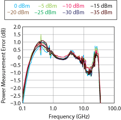
Figure 3 Detector response vs. frequency and input power, relative to 5.8 GHz.
The ground-signal-ground configuration of the RF input (see Figure 2) is designed to interface seamlessly with a coplanar grounded waveguide on a 5-mil thick RO3003 or similar substrate, without needing any external matching components. The response of the LTC5596 hardly changes over a wide input frequency range. This minimizes the need for calibration of the response at different frequencies. As shown in Figure 3, the measurement error due to the frequency response relative to 5.8 GHz is less than ±1 dB from 200 MHz to 30 GHz.
In many applications, the power levels of RF signals are typically specified on a dB scale. One motivation for this is that transmission path loss is approximately linear in dB vs. distance. The LTC5596 generates a (DC) output voltage proportional to the average power level (i.e., the RMS signal level) in dBm at its input port. The response is also very stable over a wide operating temperature range, with typically less than ±1 dB error over the full operating temperature range (see Figure 4).
At any point within the LTC5596’s dynamic range from ‐37 to ‐2 dBm, a 1 dB change in input power results in a 29 mV change of the output voltage. Diode-type detectors or linear-in-volt power detectors, for example, produce a much smaller output signal change for a 1 dB power step at low input power levels vs. high power levels. This makes it very difficult to achieve accurate power measurements over the full dynamic range. By connecting an analog-to-digital converter (ADC) to the LTC5596 output, a digital representation with constant and high resolution across the entire dynamic range of the measured power can be obtained.
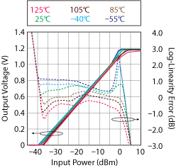
Figure 4 Output voltage vs. input power and temperature at 30 GHz, with linearity error relative to an ideal transfer curve at 25°C.
The LTC5596 also provides a simple means to apply additional filtering to the output signal, which is useful to reduce residual high frequency ripple and noise. The bandwidth of the output driver amplifier inside the device can easily be reduced with a single capacitor connected between OUT and FLTR (see Figure 2), without compromising the current drive capability. A few tens of pF capacitance is typically sufficient. Alternatively, a filter can be connected to the OUT interface of the device. The high output capability of the LTC5596 drives a wide range of impedance levels without changing power measurement accuracy. The LTC5596 is well suited for low duty-cycle applications, where the device is active only for a small fraction of the time. The output interface becomes a high impedance during shut down, which minimizes the discharge of large capacitors in an output filter and ensures fast settling once the device is enabled again.
The LTC5596 is offered in a small 2×2 DFN-8 package in I-grade (‐40° to +105°C case temperature) and H-grade (‐40° to 125°C case temperature). The H-grade also has tighter limits guaranteed for the logarithmic slope and intercept parameters, which simplifies or even eliminates the need for factory calibration.
Linear Technology Corp.
Milpitas, Calif.
www.linear.com