
Automated optimization algorithms, like the generic algorithm (GA), offer many advantages for design purposes. However, one of the drawbacks is that the methods typically do not bring much understanding about the design interactions and dependencies. This might be particularly important when design goals are not all achieved, requiring a trade-off analysis and a compromise in performance. Characteristic mode analysis (CMA) can be an extremely useful design tool in such situations. In addition, it is instrumental in answering much broader design questions like: which is the most suitable antenna for a particular application?
CMA enables a systematic design approach that is based on insight into the fundamental resonance behavior of the structure. This makes it well suited to solving challenging antenna design and antenna placement problems. The modal current and modal significance can aid in the choice of the antenna type and placement locations on the structure. CMA is also well suited to MIMO applications, where the fact that the modes are inherently orthogonal can be exploited to improve decoupling between antenna elements. This article will briefly review CMA parameters and typical workflows before presenting a smartphone antenna design example.
CMA OVERVIEW
Characteristic modes are defined as a set of orthogonal current modes that are supported on a conducting surface. The Eigenvalue equation is derived from the Method of Moments impedance matrix.1 One of the major advantages of CMA is that the analysis can be performed before any decisions are taken about the placement of any sources. The following offers a brief review of calculated CMA parameters.
MODAL RESONANCE
The eigenvalue (λ), modal significance (MS) and the characteristic angle (CA) are measures of how resonant a mode is. A mode is resonant when λ = 0, MS = 1, CA = 180°. These three quantities essentially express the same thing in different ways; which one is used depends on personal preference. If a mode is resonant on a structure, it means that it is more likely to be excited at that frequency. Conversely, a mode with a large Eigenvalue will be more difficult to excite than a mode with a smaller Eigenvalue. Note that it is not necessary to include an excitation in the CMA simulation in order to calculate these parameters, they are determined purely by the geometry and frequency of the analysis, and are independent of the excitation.
MODAL CURRENT AND FIELDS
Modal currents and fields are calculated for each mode, which is used to calculate the near field and radiation pattern of each mode. The current distribution, near field and radiation patterns of each mode can be extremely useful. From a design perspective, during a CMA study, geometry can be modified to bring a specific mode into resonance because it has desirable modal current/field/pattern attributes. Furthermore, when multiple modes are resonant, a synthesis of these parameters can be applied to predict the total current/fields/pattern.
MODAL EXCITATION AND WEIGHTING COEFFICIENT
When a coefficients excitation is included in the CMA, two additional parameters are available. The modal excitation coefficient is a measure of how well the excitation can excite a specific mode, while the modal weighting coefficient is a measure of the overall modal presence generated by the excitation. These parameters offer a useful measure of how well a design is able to excite a specific mode or combination of modes.
TYPICAL CMA WORKFLOWS
Figure 1 shows an idea of typical workflow associated with a CMA design study and the steps are described in more detail below.
Understand the structure – the first step involves the initial investigation to understand the behavior of the structure. A simplified but representative structure can be used and the excitation and antenna geometry can be excluded at this stage. The CMA analysis will determine which modes are naturally in or near resonance within the frequency range of interest and whether or not the attributes of a single mode or a combination of modes are suitable for the application at hand.
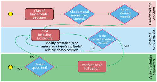
Figure 1 A typical workflow for a CMA design study.
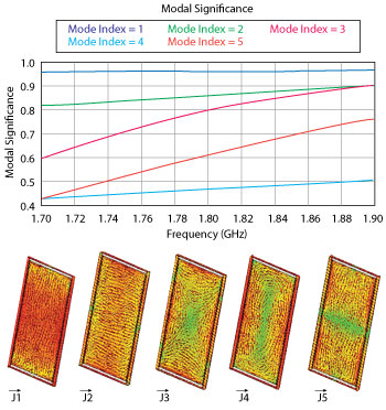
Figure 2 Initial CMA analysis of the smartphone PCB and frame showing modal significance and the modal current distributions at 1.8 GHz.
Excite the correct mode – once a mode or a combination of modes have been selected, an excitation must be designed that couples to these modes. Detailed CMA analysis of the structure and antenna(s) is performed and can determine: choice of appropriate antenna type and location, type and location of antenna feed, and in the case of multiple antennas, the amplitude and phase of the excitations. Through evaluation of the modal weighting coefficient the analysis will determine how well the design was able to achieve the selected modal behavior.
Verify the design – the final step involves a verification stage where for example a different solver is used to calculate performance parameters, e.g., S-parameters, gain, etc.
The case study that is presented in the following section will highlight how these steps can be applied by considering a practical design example.
SMARTPHONE ANTENNA DESIGN
In this example, a CMA solver2 is used to design an antenna for a modern smartphone with a 70 mm × 130 mm PCB. The antenna will be designed to operate in the DCS1800 band, where more resonant modes are present than in the lower GSM900 band3, and will be integrated directly into the outer metallic frame of the device. Several design scenarios were investigated, three of which are presented here to highlight specific aspects of how CMA can be applied.
A single antenna element is used in this example, which makes it more challenging to excite and control modes.4 In order to control the modal behavior without adding additional antenna elements, a combination of ground connections, slots and passive resonators are used in the designs.
It is worth noting that automated optimization was not used on any of these designs. All results were obtained by interpreting the CMA results, and where necessary, further design iterations were made to tweak performance. Herein lies the strength of CMA: insight that leads to informative design decisions.
Understanding the Structure – An initial CMA analysis of the PCB and frame is carried out over the frequency band of interest (1.7 to 1.9 GHz) to assess the resonant modes and the associated modal current distributions (see Figure 2). Modes 1 and 2 exhibit dipole-like characteristics with the modal current flowing along the length/width of the PCB and the frame, while modes 3 to 5 have more complex modal current distributions.
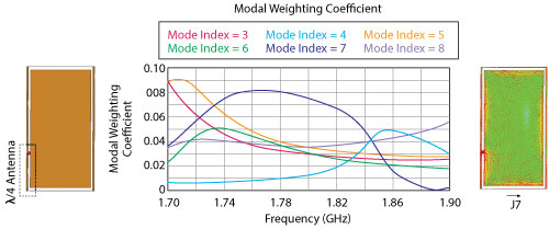
Figure 3 Quarter-wavelength design with a capacitive element to excite the dominant mode 7.
The goal is to develop an antenna which naturally couples to specific modes (with appropriate radiation patterns) on the PCB, thus improving the overall performance by incorporating the PCB as part of the antenna. Dipole-like mode 1 is near-resonance throughout the whole frequency band, and also has a suitable modal far-field pattern, making it a good candidate for this application.
Excite the Desired Modes – In the next step, the antenna geometry is included in the CMA. In addition to the modal currents and modal significance, the modal weighting coefficients are now used to measure how well each of the designs excited the desired modes. Three different designs are presented: Design 1 uses a capacitive excitation element, Design 2 clearly shows how CMA can be applied to improve a design, and Design 3 illustrates the relationship between the modal and actual bandwidth.
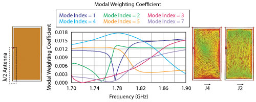
Figure 4 Half-wavelength design iteration 1.
Design 1: Quarter-Wavelength Resonator – The CMA design approach4 shows how antenna elements can be designed to excite specific modes. This approach is used to design a capacitive quarter-wavelength antenna integrated into the frame, which couples strongly to the dominant dipole-like mode running along the PCB length. However, because a single antenna is used it is more difficult to enforce the modal boundary, and the modal current distribution of the dominant dipole-like mode (see Figure 3) exhibits some distortion on the opposite side of the PCB.
Due to the distortions, this mode is automatically assigned mode number 7. Looking at the modal weighting coefficients, it is noted that mode 7 is dominant throughout most (but not all) of the required bandwidth and that several other modes are also excited. The changes in the modal weighting coefficients with frequency implies that the total radiated pattern will differ at different frequencies within the band.
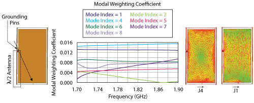
Figure 5 Half-wavelength design iteration 2, with grounding pins used to suppress the anti-resonance in the dipole-like mode.
Design 2: Half-Wavelength Resonator – Iteration 1 – A similar approach to Design 1 is applied, however a half-wavelength antenna is now used (the advantage being that this design can easily be extended to dual-band GSM900 and DCS1800 operation). Because the half-wavelength resonator is longer, the modal boundary is not enforced well and mode 4 is excited more than the desired dipole-like mode (see Figure 4). The modal weighting coefficients also show several modes come into and out of resonance, which is likely to result in suboptimum bandwidth performance.
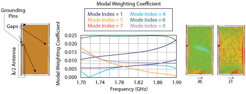
Figure 6 Half-wavelength design iteration 3 – gaps are used to suppress the frame resonance.
Iteration 2 – The first step to improve this design is to remove the anti-resonance (around 1.75 GHz in Figure 4) in the dipole-like mode to improve the radiation pattern and bandwidth performance. This is achieved by introducing grounding pins connecting the frame to the PCB opposite the antenna feed and at the lower PCB edge.
The pin opposite the antenna feed facilitates the current flowing down the long frame edge, while the pin at the lower edge introduces a passive resonator, both of which improve the excitation of the dipole-like mode. From the modal weighting coefficients (see Figure 5); we can now see that modes 4 and 1 are dominant with good bandwidth performance and that the anti-resonance has been removed.
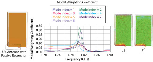
Figure 7 Narrow band design with passive resonator.
Iteration 3 – It is noted that the presence of dominant mode 4 in iterations 1 and 2 could be caused by a resonance in the outer frame (seen in the mode 4 current distribution in Figure 5). The next step to improve the design is to suppress mode 4, which is achieved by introducing gaps in the frame to break the resonant current path. From the modal weighting coefficients (see Figure 6), we now see that mode 4 has indeed been suppressed, the dipole-like mode 1 remains and mode 6 is now excited. The modal weighting coefficients of the dominant modes are relatively constant across the band, resulting in good overall bandwidth performance.
Design 3: Narrowband Design – This design uses a quarter wavelength antenna, as in Design 1, but oriented along the short edge of the PCB. A resonant slot and grounding pins are also used. In this case, both orientations of the dipole-like modes are excited (see Figure 7) leading to very good performance. However, the solution is band limited and only covers a small frequency range at the center of the band.
The next section shows how the modal weighting coefficients relate to the actual bandwidth, which is a very useful concept. Bandwidth performance can be estimated before impedance matching, which can be considered in a later stage, either through rigorous optimization or including a matching circuit.
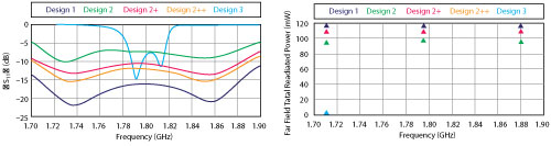
Figure 8 The |S11| and total radiated power for the different designs.
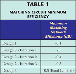
Comparing the Designs – As a means of comparison, matching circuits were generated for each design using Optenni Lab5 and the S-parameter and radiation pattern performance was simulated for each design. Due to the bandwidth constraints of Design 3, a band limited (1.785 to 1.815 GHz) matching circuit is designed to enable a meaningful comparison at the center frequency. The other designs are all matched across the full band. Table 1 shows a comparison of the efficiency of the matching networks designed with Optenni Lab, while Figures 8 and 9 show the |S11|, total radiated power and radiation patterns for the different designs.
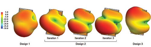
Figure 9 The total radiation pattern for each design at 1.8 GHz.
While Design 1 offers the best performance for this application, it was also demonstrated how CMA was applied to improve Design 2 performance. Furthermore, Design 3 illustrates how a CMA solution with good modal performance over a narrow frequency range will result in a narrowband design. Finally, the total radiation patterns in Figure 9 can also be calculated by superposition of the weighted modal patterns.
CONCLUSION
CMA offers a novel approach to address design challenges: insight into the inherent resonant behavior of the structure facilitates innovative design approaches. This article briefly introduced concepts and parameters that form part of a CMA analysis. A typical workflow was broken down in three main steps, which were then illustrated in more detail by means of a design example. Different design scenarios were illustrated to highlight the advantages of applying CMA as a design tool.
References
- D. Ludick et al., “Characteristic Mode Analysis of Electromagnetic Structures,” EuMW 2015.
- Altair Engineering Inc., “FEKO Suite 14.0,” Troy, MI, www.altairhyperworks.com/product/FEKO.
- P. Futter et al., “Simulation Approach for MIMO Antenna Diversity Strategies,” EDICON China 2015.
- R. Martens, et al., “Inductive and Capacitive Excitation of the Characteristic Modes of Small Terminals,” Loughborough Antennas & Propagation Conference 2011.
- Optenni Lab version 3.3, Optenni Ltd., Espoo, Finland, www.optenni.com