
Positive Bias GaAs Multithrow Switches with Integrated TTL Decoders
Hittite Microwave Corp.
Chelmsford, MA
Distribution and reception of digital, video and voice information has become an essential part of our daily routine. We use a network of fiber-to-RF cable to communicate with family, friends and coworkers via the Internet; microwaves via satellites and terrestrial links bring us voice and digital video broadcasts; and cellular and PCS telephones keep us connected just about anywhere. RF and microwave technologies have become an indispensable part of the backbone of this information infrastructure. Switching and routing information is and will always be a necessary function in these communication networks.
As consumer demand for cellular/PCS, cable modem, direct broadcast satellite (DBS), local multipoint distribution service (LMDS) point-to-multipoint and satellite data services grows, so does the demand for more advanced infrastructure switching solutions. Whether on a tower or pole, in a spacecraft or mounted to the ceiling in a mall, this new equipment requires more switching in a smaller area with less power consumption. As information becomes more complex, the demand for bandwidth increases, requiring the minimization of switch junction parasitic capacitances and inductances found in traditional discrete switch layouts. Likewise, high channel-to-channel isolation becomes important to eliminate interference.
GaAs MMIC SP4T switches with integrated decoder drivers were introduced by the company four years ago. (In the past three years, SP6T and SP8T switches have been introduced as well.) These first SP4T products required a negative bias (Vee = –5 V) and two GaAs switch logic control inputs of 0/–5 V. At the time the switches offered reduced size, control logic and improved bandwidth over other manufacturers’ products requiring up to eight control lines for an SP4T at four-times the package area. The original HMC family of negative bias SP4T, SP6T and SP8T switches with integrated decoders are now used in cellular/PCS base transceiver station antenna and filter switching, cable modem headends and DBS low noise block (LNB) switching. Emerging RF and microwave infrastructure designs demand components with wider RF bandwidth, lower insertion loss, a single positive bias supply and true TTL compatibility. A new positive bias, TTL-compatible multithrow GaAs switch line meets the new design challenges.
The Positive Bias SPNT Multithrow Product Family
The HMC241QS16 SP4T, HMC252QS24 SP6T and HMC253QS24 SP8T positive bias nonreflective switches with integrated decoders are the recent product additions. Volume production of these integrated decoder negative bias SPNT products has allowed the company to optimize their RF/digital designs for the next generation of positive bias products. These new GaAs SPNT MMIC switches feature wideband operation from DC to 3.5 GHz, covering all cellular/PCS (450 to 2000 MHz), wideband CDMA (W-CDMA) (2000 to 2300 MHz), wireless local loop (WLL) (3500 MHz), industrial, scientific and medical (900 and 2400 MHz), and CATV/DBS (50 to 2150 MHz) bands. In addition, the switches offer a single positive bias and true TTL/
CMOS compatibility in standard plastic surface-mount technology (SMT) packages (the smallest available, saving cost and size). The switches incorporate on-chip logic decoders and drivers that reduce bill of materials cost, PCB area and design time. Performance-wise, the devices provide high isolation (30 to 50 dB) and low insertion loss (0.5 to 1.0 dB) with specifications guaranteed over the temperature range of –40° to +85°C. Table 1 lists the significant characteristics of the HMC241QS16 SP4T, HMC252QS24 SP6T and HMC253QS24 SP8T nonreflective switches with integrated decoders.
|
Table I | |||
|
|
SP4T Non-reflective |
SP6T Non-reflective |
SP8T Non-reflective |
|
Part number |
HMC241QS16 |
HMC252QS24 |
HMC253QS24 |
|
Frequency range |
DC to 3.5 |
DC to 2.5 |
DC to 2.5 |
|
Insertion loss/isolation |
0.5/38 |
0.8/40 |
1.0/35 |
|
Control lines/logic type |
2/positive TTL |
3/positive TTL |
2/positive TTL |
|
+Vdd power consumption |
+5 V at 4 mA |
+5 V at 5 mA |
+5 V at 6 mA |
|
Package type |
QSOP16 |
QSOP24 |
QSOP24 |
|
Package area (sq in (sq min)) |
0.045 (29,40) |
0.080(33,54) |
0.080(33,54) |
Positive Bias SPNT Product Evolution
Prior to the introduction of MMIC switches, multithrow switch designs made use of multiple PIN diodes. To realize a single-pole eight-throw switch, up to 16 diodes and numerous inductors, resistors and capacitors were required to achieve good isolation and minimal loss. Alternatively, cascaded multithrow hybrid switches could also perform the function but at a cost to power consumption. These approaches also yielded numerous control lines and components, reduced isolation due to control line crosstalk and limited bandwidth due to parasitic junction losses.
With the introduction of commercial negative voltage control GaAs SPDT MMIC switches 15 years ago, multithrow PCB layouts were simplified over PINs and hybrids, but were still large. SP4T GaAs MMIC switches were introduced later in either wide-body SOIC24 or PLCC28 packages, making incremental progress. These switches still required up to eight negative GaAs logic control lines or dual ±5 V bias supplies while occupying an area of 0.5 inch (12.7 mm) square or larger.
The original line of negative bias SPNT switches, which includes the HMC165S14 SP4T, HMC182S14 SP4T, HMC172QS24 SP6T and HMC183QS24 SP8T, offered customers a PCB area savings of one-third and only two to three control lines vs. four to 16 for other available switches. Figure 1 shows the size and package evolution of the plastic GaAs MMIC SP4T switch. The new positive bias HMC241QS16 model offers an SP4T solution that is one-fifth the area of other versions with fewer control lines and better RF insertion loss and isolation performance as listed in Table 2 . These switches provide the lowest power consumption for a multithrow switch while offering the only specification guarantee over temperature. To date, there is still no commercially available device equivalent to either the original negative bias SP6T and SP8T switches or the new positive bias HMC252QS24 SP6T and HMC253QS24 SP8T switches.
|
Table II | |||
|
Switch Attribute |
Wide Body SOIC SP4T |
PLCC SP4T |
HMC241QS16 SP4T |
|
Frequency Range (GHz) |
DC to 3 |
DC to 3 |
DC to 3.5 |
|
Insertion Loss (dB) |
1.6 |
1.3 |
0.5 |
|
Isolation (dB) |
33 |
33 |
35 |
|
Return Loss (dB) |
12 |
14 |
20 |
|
Bias Supply (s) |
+5 V at 4 mA |
+5 V at 3 mA |
+5 V at 4 mA |
|
Control Lines |
4 |
4 |
2 |
|
TTL compatible |
yes |
no |
yes |
|
Package type |
24 lead wide-body |
28-lead PLCC |
16-lead narrow body QSOP |
|
Dimensions (L x W x H) |
0.606" x 0.407" x 0.098" |
0.409" x 0.409" x 0.173" |
0.193" x 0.236" x 0.061" |
|
Area |
0.247 sq. (158.5 sq. mm) |
0.240 sq. (156.3 sq. mm) |
0.046 sq. (158.5 sq. mm) |
|
Guaranteed specifications vs. temp. |
25°C only |
25°C only |
-40° to +85°C only |
General Product Design and Performance
All of the positive bias SPNT switches are fabricated on a standard commercial 0.6 mm enhancement/depletion (E/D) GaAs MESFET process. Therefore, they share the same design and logic interface characteristics. All decoder logic is integrated onto the MMIC chip, resulting in a true RF/digital IC. Depletion-mode MESFETs are arranged in various series and shunt configurations to achieve the desired RF switching circuit. E/D-mode MESFETs are used for the low power decoder/driver TTL to GaAs switch logic.
Off-state 50 W terminations are realized by switching a load at the RF1 to RFn inputs/outputs. The shunt switch MESFET terminal potentials are floated to +5 V DC utilizing capacitors and bias resistors connected to Vdd on chip. This technique allows the control lines to be directly compatible with positive bias TTL and CMOS drivers over the –40° to +85°C temperature range. A logic 0 is equal to 0.0 to +0.8 V DC while a logic 1 is equal to +2.0 to +5.0 V DC. The Vdd supply is +5.0 V DC ±10 percent.
All control, bias and RF ports have been designed and characterized to pass the JESD22-A114-A electrostatic discharge test method. The RF inputs/outputs are bidirectional and require DC blocking capacitors on the user PCB to achieve optimal performance at the respective frequency of operation. All of the devices may be used in 50 or 75 W systems. Products are 100 percent tested for DC and RF parameters utilizing automated test handlers.
SP4T Performance
The model HMC241QS16 SP4T requires only +5 V bias at 4 mA and two positive voltage TTL-compatible control lines via an integrated 2:4 decoder. RF1–RF4 ports are nonreflective in their off states. Figure 2 shows the unit’s insertion loss, return loss and isolation across the wide DC to 3.5 GHz specified frequency band. This device is the only SP4T MMIC switch that addresses the needs of the 3.5 GHz WLL. With only 0.5 to 1 dB insertion loss and better than 15 dB return loss through most of the band, this device can be easily cascaded to form sophisticated matrices and filter switching banks.
  Isolation between ports is greater than 40 dB in the 900 MHz cellular band and greater than 25 dB through the 3.5 GHz WLL band. An input third-order intercept point of +43 dBm provides low distortion switching for applications that demand a high dynamic range such as CDMA and W-CDMA. Figure 3 shows a functional diagram of the HMC241QS16 switch and relative pinouts in the industry-standard QSOP 16-lead SMT package.
SP6T Performance
The model HMC252QS24 SP6T requires only +5 V bias at 5 mA and three positive voltage TTL-compatible control lines via an integrated 3:6 decoder. RF1–RF6 ports are nonreflective in their off states. Figure 4 shows the unit’s insertion loss, return loss and isolation across the DC to 2.5 GHz specified frequency band. This product easily solves multiport switching problems through the new W-CDMA band of 2000 to 2300 MHz with less than 1 dB of loss and greater than 18 dB of return loss. Receive antenna switching matrices for multiple-element cellular/PCS antenna configurations can be constructed for
  six- to 24-element arrays utilizing SP6Ts. More than 33 to 40 dB of isolation between ports will satisfy DBS LNB channel-to-channel separation through 1450 and 2150 MHz. An input third-order intercept point of +40 dBm provides low distortion switching for applications that demand a high dynamic range such as CDMA and W-CDMA. Figure 5 shows a functional diagram of the HMC252QS24 switch and relative pinouts in the industry-standard QSOP 24-lead SMT package.
SP8T Performance
The model HMC253QS24 SP8T requires only +5 V bias at 6 mA and three positive voltage TTL-compatible control lines via an integrated 3:8 decoder. RF1–RF8 ports are nonreflective in their off states. Figure 6 shows the switch’s insertion loss, return loss and isolation across the DC to 2.5 GHz specified frequency band. This SP8T product has 1 to 1.8 dB of insertion loss and 30 to 45 dB of worst-case port-to-port isolation. Highly complex m ¥ n switching matrices can be achieved utilizing this SP8T switch. The input
 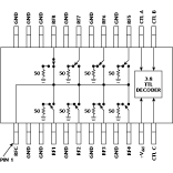 third-order intercept point is +40 dBm. Figure 7 shows a functional diagram of the HMC253QS24 device and relative pinouts in the industry-standard QSOP 24-lead SMT package. Figure 8 shows the
 SP8T evaluation PCB used for characterization and sampling purposes. Similar evaluation PCBs are available for the HMC241QS16 SP4T and HMC252QS24 SP6T devices.
The HMC253QS24 SP8T product masters the art of filter switching at both the IF and RF frequencies of cellular/PCS, cable modem, LMDS (IF) and other wideband communication receiver systems. Several approaches can be used to realize an eight-element switching matrix. The first configuration requires up to 32 PIN  diodes (16 series/shunt pairs) plus discrete capacitors, resistors, chokes and logic drivers. The brute-force MMIC approach uses 14 SPDT switches plus logic drivers. Using only four SP4T MMIC switches plus two SPDT switches merely simplifies the problem vs. the elegant two-SP8T switch configuration, which utilizes two HMC253QS24 SP8Ts, as shown in Figure 9 .
Conclusion
Three new multithrow GaAs switch products have been introduced that will help wireless infrastructure designers improve their system size, performance, reliability and production margins. The introduction of the positive bias HMC241QS16 SP4T, HMC252QS24 SP6T and HMC253QS24 SP8T nonreflective switches with integrated decoders advances the state of the art in MMIC switching. Improvements have been demonstrated in bandwidth, insertion loss, isolation, power consumption, logic interface and size over previous available products. These new products are based upon standard MMIC wafer processes and industry-standard plastic packages and assembly techniques, and are 100 percent RF/DC tested utilizing high speed auto-handler test stations.
Hittite Microwave Corp.,
Chelmsford, MA
(978) 250-3343.