
LTCC-M: An Enabling Technology for High Performance Multilayer RF Systems
B. Geller, B. Thaler, A. Fathy, M.J. Liberatore, H.D. Chen, G. Ayers, V. Pendrick and Y. Narayan
Sarnoff Corp.
Princeton, NJ
Over the last several years, the highly competitive wireless market has pushed manufacturers of RF hardware toward the development of products with more functions in a smaller volume, operation at ever higher frequencies, and greater circuit and functional integration. Additionally, the pressure to reduce costs has forced designers to consider less expensive manufacturing, assembly and testing techniques.
One fairly direct way to accommodate this drive is to switch from what has traditionally been a two-dimensional printed circuit environment to a three-dimensional environment. Multilayer RF technology has the potential to not only allow greater functional density, but to do so with low cost, good performance, high reliability and good reproducibility. Although different approaches are available for the realization of multilayer circuits, including various systems based on organic or soft boards and high temperature ceramics, the low temperature cofired ceramic (LTCC) approach has the greatest potential for meeting a wide range of system performance, cost and manufacturability requirements.
However, in its basic version, LTCC suffers from two major drawbacks. First, the ceramic shrinks in all three dimensions during the firing process. This shrinkage limits the size of the boards that can be processed, imposes limitations on embedded passive components and introduces complexity in the processing of boards with cavities. In addition, modules requiring heat removal must have a heat spreader attached after firing.
The LTCC-M
In order to address many of these problems, an improved LTCC on metal (LTCC-M) technology has been developed in which a specially formulated multilayer ceramic structure is attached to a metal carrier or core. The ceramic firing and core attachment processes occur in the same step. The resulting structure exhibits virtually no shrinkage in the substrate plane. All of the shrinkage is constrained to the Z dimension (normal to the plane of the substrate) and is predictable and uniform.
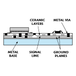 Figure 1 shows the cross section of a basic single-sided LTCC-M board. Layers of unfired or "green" tape are punched and patterned with the required conductors and other passive components. The layers are then stacked and laminated and the multilayer stack is attached to the metal base and fired. The fabrication process is straightforward and relatively inexpensive to implement.
Figure 2 shows a flow chart of the basic process. The process allows the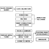 inclusion of buried resistors and overlay capacitors covering a wide range of values as well as vias and planar conductor patterns such as transmission lines and spiral inductors. The virtual absence of shrinkage in the X-Y plane allows the fabrication of relatively large area boards with good layer-to-layer registration and alignment accuracy.
Depending on the application, several metals can be used for the core. Two systems have been developed for RF applications: one based on a Cu-Mo-Cu laminate and the other on Kovar. The Cu-Mo-Cu core is preferred for applications in which maximum heat spreading capability is required. Both systems have expansion coefficients that are compatible with GaAs, allowing the mounting of bare die directly on the heat spreader.
A significant amount of recent work, mostly under US Defense Advanced Research Projects Agency (DARPA) funding, has been performed to extend and improve the performance and capabilities of the LTCC-M Cu-Mo-Cu system. Table 1 lists the system's key electrical, mechanical and thermal properties.
|
Table I | |
|
Firing Temperature (°C) |
875 to 925 |
|
Dielectric constant |
|
|
Dielectric loss tangent at 15 GHz |
0.001 |
|
Volume Resistivity ( - Wcm) |
5x10-15 (25°C) |
|
Thermal Coefficient of Expansion |
56 x 10-7 /°C (25°C) |
|
Substrate camber (in/in) |
0.002 |
|
Shrinkage (%) |
|
|
Surface roughness (nm CLA) |
|
|
Ag conductor sheet resistance (m W/sq) |
3 to 8 |
|
Number of layers |
15+ |
|
Coefficient of thermal expansion Cu/Mo/Cu (13/74/13 ratio) |
55 x 10-7 /°C |
|
Thermal conductivity (W/m-°C) |
|
|
Core thickness (mils) |
5 to 40 |
 The RF properties of the LTCC-M ceramic have been characterized up to approximately 40 GHz. Figure 3 shows the loss (in decibels per inch) of 50 W microstrip transmission lines on 0.010- and 0.025-inch-thick LTCC-M substrates. A standard thin-film gold conductor was used to compare the properties of the LTCC-M to those of alumina. As a comparison, the figure also includes the expected loss of a 0.010-inch-thick alumina substrate. The losses are virtually the same, indicating that the circuit losses are dominated by the ohmic metal loss rather than the ceramic.
Both the Kovar and Cu-Mo-Cu systems use thick-film silver conductor metal,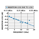 which has the benefits of good conductivity and the ability to be fired in an air atmosphere. Figure 4 shows the measured RF losses of a 4-cm-long microstrip line on the Cu-Mo-Cu LTCC-M using the thick-film silver conductor. The measured data were linearly extrapolated to 20 GHz and indicate a loss of approximately 0.13 dB/inch at low frequencies, 0.35 dB/inch at 10 GHz and 0.55 dB/inch at 20 GHz.
A series of thick-film inks were developed to span the range of embedded resistor and capacitor requirements. The buried passive component specifications were drawn from both commercial and military wireless communications products. Specifically, inks having dielectric constants of 10, 40, 60, 500, 1000 and 2000 were developed and exhibit low temperature coefficients of capacitance, which allow integrated capacitors to span the range from 0.2 to 50,000 pF. Typical capacitor tolerances are currently in the range of ±10 to 20 percent.
A series of buried resistor ink compositions based on RuO2-glass mixtures were also developed to meet system requirements. Specifically, inks having sheet resistivities of 40, 100, 200, 750 and 12,000 W/square were developed and exhibited low temperature coefficients of resistance. Typical buried resistor tolerances are currently in the range of 15 to 25 percent range. Resistor divider networks (~ 5:1 ratio) have been fabricated with the 200 W/square ink and have exhibited a resistor ratio tolerance of ±5 percent. LTCC-M substrates and their integrated components have been subjected to long-term accelerated aging tests such as temperature-humidity-bias storage (at 85°C, 85 percent relative humidity, 50 V bias across capacitors) and thermal shock (-55° to +125°C) without any degradation in their electrical or mechanical properties.
The LTCC-M Design Kit
A design kit for the simulation and layout of multilayer LTCC-M substrates containing embedded lumped passive components, surface transmission lines and embedded transmission lines has been developed to make this technology more accessible. This user-friendly software works with the industry-standard Hewlett-Packard (HP) Communications Design Suite (CDS) Series IV and offers custom menus and dialog boxes. The design kit software incorporates a materials file that acts as a central storage point for all material and process parameters (ceramic dielectric constant, ink parameters, LTCC-M-specific design rules, etc.) and is used as the central reference file for designing all passive components. Technology enhancements can be incorporated by simply modifying the materials file, thus making the design kit easy to upgrade.
The design kit has LTCC-M-specific CAD models for embedded resistors, embedded capacitors, inductors and surface/embedded transmission lines (microstrip lines, covered microstrip lines and striplines). These CAD models enable the CDS to function in a multilayer environment and support integrated passive components. The CAD models were verified by fabricating and testing LTCC-M test coupons for embedded resistors and capacitors, surface inductors, and surface and embedded transmission lines (microstrip lines, covered microstrip lines and striplines). Measured results were compared using electromagnetic (EM) simulation and the models were optimized. Two auxiliary tools (written in platform-independent JAVA) were developed: a component synthesis tool that allows the designer to synthesize physical LTCC-M components, and a cross-section visualization tool that allows the designer to visualize the multilayer structure.
Passive Component Simulation
Models were developed and verified for embedded overlay capacitors, resistors and inductors. The model uses components with physical attributes such as width and length, and then all relevant dimensions are calculated based on design rules specific to LTCC-M.
Capacitors
 Models were verified theoretically and experimentally with good agreement. Figure 5 shows an example of the validation of the LTCC-M capacitor circuit model using EM simulation. Good agreement between the circuit model and measured results is demonstrated. As an example, for the high value dielectric inks where the circuit model parameters are based on average measured values of the fabricated capacitance per unit area, circuit models can be closely fitted to the measured results by optimizing the ink dielectric constant and thickness.
Resistors
Resistors were fabricated and tested from DC to approximately 4 GHz.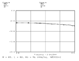 Resistors in the range of one-half to three squares and 30- to 35-mil width can be controlled to values within ±15 percent. Using the HP CDS libraries, an RF circuit model for the buried resistors was developed. This model was validated with EM simulation and compared to measured results for various resistor sizes, as shown in Figure 6 ; good agreement was found. A slight deviation of the measured results in comparison with the modeled results could be seen, especially for the extreme resistor sizes, and can be attributed to screen printing nonuniformity.
Inductors
The HP library model for square spiral inductors has been validated experimentally. This model takes into account the mutual-inductive-coupling to all other parallel segments, including those of an image spiral, to account for the effect of the ground plane. The effect of the underpass is also taken into consideration.
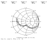
 Spiral inductors have been fabricated using eight- and four-mil lines and spaces on a 15-mil substrate where a maximum inductance of 90 nH was achieved with a 260-mil square spiral. The measured S parameters of various inductors are shown in Figure 7 . Good agreement between measured and modeled results was obtained up to frequencies very close to the self-resonant frequency of these inductors. A peak Q value of 40 at 1.32 GHz for a 4.8 nH 8-mil spiral inductor was obtained. Other LTCC-M processing techniques to further increase these Q values are being developed.
 The design kit has the look and feel of the standard HP Series IV product. Figure 8 shows the look of a schematic entry window containing LTCC-M components. Figure 9 shows a layout window
 illustrating one of the circuit layers.
This technology has already been successfully demonstrated under DARPA programs in both digital and microwave applications. The LTCC-M technology has been transferred to a merchant supplier, Dielectric Laboratories Inc. (DLI). Through its DiPak product line, DLI has established a manufacturing facility and entered the LTCC-M ceramic package and substrate market.
Applications
Applications of LTCC-M technology range from single-cavity packages for semiconductor die to complex modules with buried passive components. The three examples discussed here (fabricated at DLI) illustrate the wide range of applicability of the current LTCC-M technology.
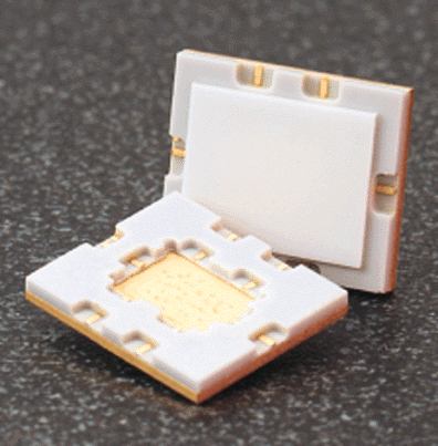 Figure 10 shows a high frequency package designed to operate up to 40 GHz. The transition in the M 20001 package has a return loss of approximately 20 dB at 40 GHz and a maximum insertion loss of approximately 0.23 dB at 40 GHz.
Figure 11 shows an example of an integrated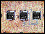 multichip module that includes integrated passives. The application is a miniaturized 2 to 18 GHz amplifier and includes eight buried capacitors and two resistors. The package measures 0.70" x 0.55" with
 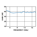 two buried circuit layers and produces 40 dB of gain, as shown in Figure 12 .
As part of the DARPA-sponsored Mixed Signal program, Sarnoff worked with TRW and DLI to demonstrate the applicability of LTCC-M technology to a direct digital synthesizer (DDS) module. The finished unit is shown in Figure 13 . The DDS operates at a clock frequency of 480 MHz and dissipates approximately 8 W.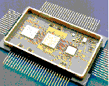 Although some surface-mounted passive components are apparent, 46 other components were integrated into the multilayer structure, substantially reducing the parts count and cost. The performance was comparable to that of the hybrid version. The size of the module could have been reduced, but the overall dimensions of the package were constrained to remain as before the integration in order to fit into an existing application.
The finished package measures 2.00" x 1.25" and consists of eight tape layers, three of which are used to form the seal ring and input/output area. Three buried layers are used for the resistors and capacitors: layer 1 (first layer up from the metal base) has seven capacitors (4700 pF), layer 2 has 23 capacitors (82 pF) and layer 4 has 16 resistors.
Future Directions
 The examples described in this article show only a glimpse of the potential of this technology. The ability of integrate complete subsystems will soon include the integration of printed antenna subsystems. Figure 14 shows a complete transmit/receive subsystem on a single LTCC-M panel. Note that a doublesided board is used in which the RF parts of the system are located on the top side (with the radiating elements), and the low frequency, DC and control functions are located on the back side. The printed panel may contain the complete antenna, which might be the case in millimeter-wave systems, or may be one of several panels to realize a larger, lower frequency (or higher gain) system. The ability to fabricate such panels in nonplanar configurations also opens up the possibility for many potential applications.
Conclusion
The future development of RF and microwave technology and its successful application to modern systems depend on the development (and utilization) of three-dimensional subsystem integration techniques. These techniques must respond to the needs of the marketplace for more functionality in less volume and at lower cost. LTCC-M is believed to be one of the best approaches to meeting these goals.
Acknowledgment
This work was sponsored, in part, by DARPA contract no. F33615-96-2-5105 and Wright Patterson Air Force Base (WPAFB). The miniaturized 2 to 18 GHz amplifier assembly was designed and assembled by Northrop-Grumman, Rolling Meadows, IL (under a DARPA/ETO-sponsored MAFET Thrust-Area-2 subcontract and monitored by Wright Laboratory, WPAFB). The authors wish to thank Bill Vitriol and Wendell Hautaniemi of DLI, Stephen Consolazio of Northop-Grumman and R. Duprey of TRW for allowing the use of their products as examples.