
Correlation between Ungated Recess Width and Linearity of GaAs MESFETs
Intermodulation distortion and adjacent-channel power ratio (ACPR1) performance of GaAs MESFET discrete and MMIC power amplifier (PA) devices has been found to be dependent on the width of the ungated recess. Devices with wide ungated recess exhibit soft gain compression and poor linearity performance. Degraded linearity for these devices is manifested in worse third-order intermodulation and ACPR1 for the same output power or power-added efficiency (PAE) and significantly different fifth-order intermodulation and alternate-channel power ratio (ACPR2) dependence on the output power and PAE. Soft gain compression leads to premature power saturation, smaller power gain and degraded PAE. ACPR1 degradation was also caused by the gain compression and not the phase distortion. Linearity degradation for wide ungated recess devices was consistently observed at different biases and matching conditions. Good correlation between the load-pull results, waveform measurements and two-stage linear PA performance was obtained. The effects of longer gate length and deeper second recess were also analyzed and determined to be insignificant compared to the width of the ungated recess. This article provides insight into a critical device parameter for optimum performance of high efficiency linear PAs.
Yevgeniy A. Tkachenko, Dylan Bartle and Ce-Jun Wei
Alpha Industries Inc.
Woburn, MA
High volume linear PA production requires a good understanding of process parameters that determine device distortion characteristics. The linearity specifications, such as third-, fifth- and seventh-order intermodulation products (IM3, IM5 and IM7), ACPR1 and ACPR2, need to be correlated with the main process parameters to ensure good control of the process and high line yields. One of the critical parameters affecting discrete and MMIC GaAs  MESFET device linearity was determined to be the width of the ungated recess (or the distance between the gate edge and the edge of the second recess), as shown in Figure 1 . The ungated recess width d affects the number of traps present at the interface between the GaAs channel and a silicon nitride passivation layer in close proximity to the gate electrode. These traps were previously reported to affect the MESFET performance via the so-called gate lag phenomenon1-3 and the change in breakdown voltage.4 While the previous work primarily emphasized analog applications, this article describes the effect of ungated recess width on the linearity of the MESFETs.
Device Technology
The device under study was a standard 0.8-mm-gate, high-low-high-doped, double-recessed MESFET used in high volume PA manufacturing. The mesa isolation step was followed by the ohmic contact formation using an AuGeNi/Au alloy. Channel and gate recesses were formed by means of optical lithography and wet chemical etching. Gates were formed by Ti/Pd/Au liftoff. The gates were placed symmetrically in the channel recess with a source-drain spacing of 4 mm. In this study, the ungated recess width d was intentionally varied from 46 to 175 nm from wafer to wafer. The MESFETs were passivated with the plasma-enhanced chemical vapor deposition silicon nitride. Metallization was plated with 3.5 mm of gold and the wafer was ground to a 4-mil thickness.
Results DC Characteristics
The high-low-high doping profile realized by molecular beam epitaxy growth produces a nearly flat Gm vs. Vgs response, which is desirable for linearity. Table 1 lists the DC parameters of the MESFETs with different d. It can be seen that Idss , Vp and transconductance Gm measured at 90 and 50 percent of Idss were quite similar, while Gm in the near pinch-off region (measured at 15 percent of Idss ) was degraded with increased d. As also indicated, breakdown voltage typically increased with d, however, it was high enough not to influence any measurements reported in this article.
|
Table I | ||||||||
|
d (nm) |
46 |
65 |
86 |
101 |
119 |
130 |
151 |
175 |
|
Idss (mA/mm) |
201 |
223 |
225 |
221 |
209 |
212 |
214 |
204 |
|
Vp (V) |
-1.7 |
-2.0 |
-2.0 |
-2.0 |
-1.9 |
-1.9 |
-2.0 |
-1.9 |
|
Gm 1 (mS/mm) |
134 |
126 |
121 |
119 |
123 |
125 |
123 |
132 |
|
Gm 2 (mS/mm) |
128 |
122 |
118 |
118 |
118 |
118 |
116 |
118 |
|
Gm 3 (mS/mm) |
97 |
96 |
95 |
93 |
89 |
89 |
87 |
85 |
|
Vbd (V) |
19 |
21 |
19 |
19 |
23 |
22 |
24 |
25 |
Load-pull Measurements: Single Tone
On-wafer single- and two-tone measurements were performed on 1 and 2 mm MESFETs using an automated load-pull measurement system.5 Typically, 1 mm devices achieve P1dB of 23.7 dBm (234 mW/mm) with associated PAE of 64 percent and small-signal gain of 20 dB at 850 MHz and 5.8 V.
Figure 2 shows a comparison of gain characteristics of the MESFETs with different d. Devices were biased at Vds = 5.8 V and Id0 = 15 mA. Fundamental source- and load-reflection coefficients presented to the devices were 0.8 Ð 24° and 0.3 Ð 73°, respectively. This matching condition was optimal for CW power and efficiency, but not for linearity.
With increased d, the small-signal gain is reduced and softer gain compression is  observed. Reduction of the small-signal gain is attributed to the reduced Gm around the bias point. This observation is consistent with an increase in gate length, which in this experiment accompanies the increased ungated recess width listed in Table 2 . As will be demonstrated, the soft gain compression is caused entirely by the wide d and is not related to increased Lg . The increase in d causes premature output power saturation, which requires additional input drive to achieve the same output power level. Figure 3 shows that PAE degrades with increased d as a result of lower power gain as expected.
|
Table II | ||
|
Wafer # |
Ungated Recess Width d (nm) |
Gate Length ( mm) |
|
1 |
46 |
0.76 |
|
2 |
65 |
0.82 |
|
3 |
86 |
0.80 |
|
4 |
101 |
0.86 |
|
5 |
119 |
0.86 |
|
6 |
130 |
0.90 |
|
7 |
151 |
0.90 |
|
8 |
175 |
0.98 |
Load-pull Measurements: Intermodulation Distortion
 Figures 4 and 5 show the measured IM3 and IM5 vs. output power per tone. (These measurements were performed at 850 MHz with 10 kHz tone spacing.) No special tuning for linearity was performed in this case and the same matching states
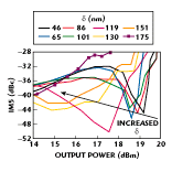 were used, which were optimal for single-tone saturated Pout and PAE. Under these conditions, a typical device with narrow d delivers a total linear output power of approximately 20.9 dBm (123 mW/mm) with PAE of approximately 35 percent and associated IM3, IM5 and IM7 of -25, -35 and -45 dBc, respectively.
IM3 remains approximately the same for 46 < d <101 nm, but worsens significantly for ds of 119 nm and higher. The change of IM5 with d (specifically its dependence on Pout) is more subtle. When d is increased from the 46 to 65 nm range to the 86 to 101 nm range, IM5 remains approximately the same for Pout > 18 dBm per tone and is slightly improved for 16 < Pout < 18 dBm per tone. For ds of 119 nm and higher, the dip in IM5 moves toward lower output powers and eventually disappears. For wide d devices, IM5 is clearly degraded for Pout around 18 dBm per tone, which is the targeted range of operation.
Linear PAs are frequently designed to utilize such a dip (or the so-called sweet spot) to minimize IM5. However, this sweet spot is very sensitive to the ungated recess d. For such a design to work properly, d must be tightly controlled.
Load-pull Measurements: ACPR1 and ACPR2 per IS-95
The biasing and matching conditions were changed for the ACPR measurements to provide the best trade-off between ACPR1, ACPR2, PAE and output power Pout . The bias current of 10 mA was chosen in an attempt to achieve ACPR1 = -48 dBc, and ACPR2 = -60 dBc while maximizing PAE. The load-pull system allowed independent tuning of the fundamental and second-harmonic load. Similar to a previously described device,6 the optimum second-harmonic impedance (in terms of ACPR1 and PAE) was found to be near the short circuit.
 Figure 6 shows ACPR1 vs. PAE characteristics of MESFETs with different d. Similar to the IM3 measurement, ACPR1 is degraded with increased d. Narrow d devices achieve PAE of approximately 50 percent at ACPR1 = -48 dBc, while the wide d
 devices demonstrate PAE of less than 35 percent at the same ACPR1 level. Figure 7 shows that the effect of d on ACPR2 is smaller than on ACPR1 and is somewhat similar to the effect on IM5. For 86 < d < 101 nm, ACPR2 is better than for 46 < d < 65 nm and, for d of 119 nm and higher, ACPR2 is seriously degraded.
 Figures 8 and 9 show that the impact of d on ACPR1 and ACPR2 comes primarily from the AM-to-AM distortion and not the AM-to-PM distortion. These measurements were performed
 under the same conditions as the ACPR measurements reported previously. The AM-to-PM responses are essentially independent of d while the gain characteristics demonstrate soft compression behavior for the wide d devices (similar to the optimum single-tone matching condition described previously).
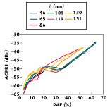 Figure 10 shows the degradation of ACPR1 with d for the 3.2 V bias. While PAE at 3.2 V is smaller than at 5.8 V, the conclusion about the effect of d remains the same. The degradation of linearity with d therefore appears independent of both biasing and matching conditions. The effect of ungated recess width was also determined to be more important than the recess
 depth. Figure 11 shows the IM3 and ACPR1 dependence on PAE for the two devices with the same d of 46 nm and different pinch-off voltages of -1.5 and -1.8 V achieved by varying the depth of the second recess. It can be seen that linearity of both devices under the same match and bias of 5.8 V and 10 mA was remarkably similar. This result highlights the importance of d as the major process parameter affecting linearity.
Gate Length Investigation
As discussed previously, the wafers with larger d also have longer gate length. 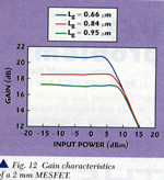 To separate the effects of increased gate length on the power saturation and linearity, wafers were processed with the same d of 45 nm and gate lengths Lg of 0.66, 0.84 and 0.95 mm. Figure 12 shows that for these wafers the small-signal gain decreased with increased Lg . Gain compression was abrupt for any Lg and, therefore, dependent only on d. Figure 13 shows that IM3, IM5
 and IM7 of the MESFETs with different Lg but the same d were very similar for all output power levels. Note that the output power at 1 dB gain compression was similar (25.8 dBm) for all three Lg values. The output power at 1 dB gain compression point frequently is associated with multicarrier linear output power. This rule of thumb applies in the case described here, however, the softness of compression and the way this 1 dB compression point is reached are also important. Thus, linearity as well as gain compression are affected only by the gate recess width d and not by the gate length.
Waveform Measurements
 To further investigate the effect of d on the large-signal performance, the output voltage and current waveforms of the MESFETs were measured
 using the Hewlett-Packard Microwave Transition Analyzer-based technique.7 Figure 14 shows the current waveforms measured at 0.85 GHz in the 50 W system; Figure 15 shows the drain voltage measured at 0.85 GHz in the 50 W system.
The bias condition was consistent with the load-pull measurements (Vds = 5.8, Id = 15 mA) and the input power was -6, 0, 6 and 12 dBm, respectively. At small input drive levels of -6 and 0 dBm, the difference between the waveforms measured for devices with different d is small. As the drive level is increased, waveforms deviate more from each other and devices with larger d exhibit more compression of both current and voltage waveforms. This change, in turn, translates into lower power gain and worse linearity as observed during the load-pull measurements.
PA Measurements
To confirm the results obtained on the discrete MESFETs, the two-stage digital PA wafers were processed with intentionally varied ds of 60, 74 and 120 nm. Compared to the small d devices, amplifiers with d = 120 nm exhibit approximately 1 dB lower output power, four percent lower PAE and more than 3 dB lower large-signal gain, as listed in Table 3 . Due to the soft gain compression, these amplifiers must be driven harder to approach the rated power performance. Large d amplifier linearity suffers significantly, especially IM3 and IM5. The results described here agree with the discrete MESFET performance.
|
Table III | |||
|
Wafer # |
1 |
2 |
3 |
|
d (nm) |
60 |
74 |
120 |
|
Lg ( mm) |
0.73 |
0.72 |
0.82 |
|
Pin (dBm) |
-2.2 |
-1.1 |
1.0 |
|
Pout (dBm) |
28.0 |
28.1 |
27.0 |
|
Gain (dB) |
30.2 |
29.2 |
26.0 |
|
PAE (%) |
38.0 |
38.6 |
34.2 |
|
IM3 (dBc) |
35.7 |
28.2 |
21.5 |
|
IM5 (dBc) |
38.4 |
37.4 |
34.1 |
|
IM7 (dBc) |
47.5 |
47.0 |
46.3 |
Conclusion
The increase in ungated recess width was determined to cause degradation of linearity and PAE of GaAs MESFETs. The degradation was manifested in lower output power and efficiency for the same IM3 or ACPR1, a shift of the dip (or the sweet spot) in IM5 and a degradation of ACPR2. The effect was especially pronounced for an ungated recess width of 119 nm and higher. The degradation is observed under both optimum single-tone power matching and optimum linearity matching conditions and at both Vds of 5.8 and 3.2 V. The effects of both increased gate length and deeper second recess etching on the linearity were determined to be insignificant compared to the increased width of ungated recess. Two-stage linear PA and waveform measurements of the discrete devices were used to confirm the result. Based on this study, process conditions were optimized and specification limits were introduced to yield high performance linear PAs.
Acknowledgment
The authors wish to thank Paul DiCarlo for his help with linear PA design and measurement and Dave Petzold for his assistance with wafer processing and scanning electron microscope measurements.
References
1. M. Rocchi, "Status of the Surface and Bulk Parasitic Effects Limiting the Performances of GaAs ICs," Proceedings of the European Solid State Device Research Conference, 1985, pp. 119-138.
2. R. Yeats, D. D'Avanzo, K. Chan, N. Fernandez, T. Taylor and C. Vogel, "Gate Slow Transients in GaAs MESFETs: Causes, Cures and Impact on Circuits," Technical Digest of the International Electron Device Meeting, 1988, pp. 842-845.
3. A. Platzker, A. Palevsky, S. Nash, W. Struble and Y. Tajima, "Characterization of GaAs Devices by a Versatile Pulsed I-V Measurement System," 1990 IEEE-MTT Digest, pp. 1137-1140.
4. H. Mizuta, K. Yamaguchi and S. Takahashi, "Surface Potential Effect on Gate-drain Avalanche Breakdown in GaAs MESFETs," IEEE Transactions on Electron Devices, Vol. ED-34, No. 10, October 1987, pp. 2027-2032.
5. LP2 User's Manual, ATN Microwave Inc., Billerica, MA.
6. Y. Tkachenko, Y. Zhao and D. Bartle, "PHEMT Technology for High Efficiency CDMA Power Amplifiers," submitted to ISRAMT '99.
7. C.J. Wei, Y. Tkachenko and J.C.M. Hwang, "Noninvasive Waveform Probing for Nonlinear Network Analysis," Microwave Journal, Vol. 37, No. 2, February 1994, pp. 122-126.