
Planar Integrated Antenna Technology
Over the last several decades, the development of planar antenna technology has fundamentally changed the microwave and millimeter-wave communication fields. Planar antennas can be printed on dielectric substrates with minimal cost and processing. In many applications, these compact and low profile antennas offer an inexpensive solution to previous generations of waveguide-or-reflector-based antenna systems. Indeed, increased penetration of commercial wireless applications at these frequencies requires all of the flexibility that this class of antennas has to offer. This article illuminates this flexibility by presenting several unique examples of planar antennas and their related design issues.
W.R. Deal, Y. Qian and T. Itoh
University of California, Los Angeles, Electrical Engineering Department
Los Angeles, CA
V. Radisic
HRL Laboratories
Malibu, CA
During the past several decades, much attention has been focused on the development of planar antennas. These antennas are highly desirable for a number of reasons. First, they can be manufactured at a much lower cost than waveguide-based antenna technology and are considerably more compact and lightweight. These characteristics are essential for the many commercial applications that planar antennas are increasingly used in, such as base station or handset antennas. Second, the planar nature of the antennas makes them ideal for large arrays and simplifies the interaction of additional electronics, such as amplifiers and phase shifters, which are essential for electronic warfare, radar, satellite communications or millimeter-wave imaging. Their planar nature also allows the antennas to be used in applications where size and shape are crucial, such as conformal printed antennas on an airplane fuselage. This myriad of applications has led to the development of a wide variety of planar antenna classes. This article attempts to classify some of these antennas and their characteristics and discuss some novel architectures and techniques that have been developed recently.
One driving factor that makes planar integrated antennas so desirable is their ease of integration with microwave or millimeter-wave circuit components. For this reason, planar integrated antennas must be compatible with these technologies, which, at microwave and millimeter-wave frequencies, are typically microstrip or coplanar waveguide (CPW) based. These transmission lines have several advantages, including the ability to integrate three-terminal devices, mechanical and heat-sinking capabilities due to metallic ground planes and simplified packaging issues. Therefore, it is essential that these types of transmission lines directly (or indirectly) feed the planar integrated antennas. Examples of direct feeding include the patch antenna and slot antenna, which are easily integrated with microstrip or CPW, respectively. Indirect feeding can include transitions or various forms of electromagnetic coupling. The method of feeding is critical and can affect antenna cross-polarization, patterns and bandwidth as well as possible array architectures.
However, the grounded dielectric slabs on which microstrip- and CPW-compatible antennas are fabricated support TM0 surface waves and can propagate energy away from the antenna in the form of surface waves, thereby lowering efficiency. While the losses are small at lower frequencies, they can be a significant problem at microwave and millimeter-wave frequencies where many new applications are targeting planar antennas. The thickness of the substrate, permittivity and frequency of operation determine the amount of surface wave losses. Several methods have been developed to reduce these losses, as will be discussed in this article.
Different classes of planar antennas are capable of a broad variety of radiation characteristics. The most common classes - patch and resonant slot antennas - demonstrate broad, low gain patterns that make them suitable for use in multi-element beamforming arrays or portable handsets. Additionally, some of these antennas can be modified easily for dual-linear or circular polarization. More sophisticated classes demonstrate higher gains and some are capable of frequency scanning.
Patch Antennas
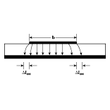 The patch antenna has several benefits. This type of antenna features a broadside radiation pattern that allows it to be integrated into two-dimensional arrays. In addition, various feeding schemes can be used to achieve linear or circular polarization. A cross section of the patch antennas is shown in Figure 1 .
A simple and intuitive technique for modeling this antenna is the transmission line model. This model assumes that the patch antenna consists of perfect magnetic conducting walls on its sides, giving rise to standing-wave-type modes inside the patch antenna cavity. The total length of the cavity is the length of the patch antenna and an effective length at each edge due to the microstrip open-end effect. The fundamental resonance of the antenna occurs at a frequency where the cavity length is one-half wavelength.
Since its length determines the resonant frequency of the patch, higher antenna resonances coincide with frequencies that are multiples of the fundamental resonance. If active circuitry (which may generate harmonic frequencies) is integrated with the patch antenna, harmonic radiation and co-site interference may occur. The circular segment patch antenna, shown in Figure 2 along with the measured input impedance, has been specifically designed to eliminate this problem.1 In this case, higher  resonances of the antenna are determined by circular harmonics (Bessel functions) and can be designed to occur away from circuit harmonics. This condition is evident from the plot of input impedance. This antenna is fabricated on low permittivity RT/Duroid. Radiation patterns of the circular segment patch antenna are shown in Figure 3 and are quite similar to a standard rectangular patch antenna. Measured cross-polarization of the antenna was better than 16 dB and gain was 5.8 dB.
Feeding is extremely important with the patch antenna. Microstrip-fed patches have very narrow bandwidths, almost invariably less than five percent. Other feed mechanisms have been used to increase bandwidth, including proximity and aperture coupling, both of which require multilayer fabrication.2
Alternatively, the antenna substrate can be made electrically thicker, effectively lowering the Q of the antenna cavity for increased bandwidth. However, high levels of TM0 surface waves can result and, therefore, reduce the radiation frequencies as well as degrade the radiation pattern if the surface wave generates radiation (which can occur at the edge of finite ground antennas). The problem of an electrically thick substrate is also common for high frequency antennas on high permittivity substrates, and high amounts of TM surface waves can result.
Several methods have been proposed to combat this problem. One method involves micromachining closely spaced holes into the high dielectric constant substrate to lower the effective permittivity in the antenna region and, therefore, reduce the electrical thickness.3-4 Although this method will increase radiation efficiency, some bandwidth may be sacrificed due to the lowered effective permittivity.
More recently, the photonic bandgap (PBG) concept has been used for this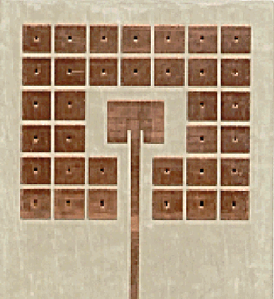 purpose. In this case, a periodic array of perturbations is used to suppress the surface-wave mode, such as the structure incorporated with an inset feed patch antenna shown in Figure 4 , which consists of capacitive pads on the top plane connected to ground by inductive shorting pins. Full-wave analysis demonstrates that this periodic structure is indeed effective at eliminating the TM0 surface wave. When integrated with a patch antenna on a 10.2 RT/Duroid substrate, it was found that the gain of the antenna increased by 1.6 dB compared to a reference patch without PBG. The integration also had the unexpected effect of increasing the bandwidth of the antenna by a factor of 3.4 to 5.4 percent.5 This increased bandwidth is believed to be due to the operation of the PBG surface as a parasitic element.
Slot Antennas
The slot antenna, comprising a narrow slit in a ground plane, is a very versatile antenna. With modification, the device is amenable to waveguide, CPW, coaxial, slotline or microstrip feeding schemes and has found application in all aspects of wireless and radar systems. The slot antenna has been investigated since at least the 1940s.6 Planar microstrip-fed slot antennas have been reported as early as 1972.7
The resonant half-wavelength slot antenna is desirable because of its compact size. However, the antenna has a large input impedance, typically larger than 300 W, which makes it unattractive to match to. This match problem can be circumvented by using an offset microstrip feed or the folded-slot antenna, which stems directly from the folded dipole by Booker's relation. In this case, the slot is folded in upon itself. The overall length of the antenna remains approximately a half-wavelength, but increasing the number of folds reduces the radiation resistance.
The CPW version of the folded-slot antenna has been investigated extensively.8-9 This antenna requires no input matching, which makes it an inexpensive and compact candidate for direct integration with microwave circuits. The broad radiation pattern also makes this antenna a good candidate for wireless communication systems, which currently are pushing into the microwave regime.
The basic structure for the microstrip-fed folded-slot antenna along with a finite-difference time-domain (FDTD) simulation of the aperture field distribution are shown in Figure 5 . The folded-slot antenna is etched in the ground plane of the substrate. One of the inner metallizations of the slot is connected to the microstrip  conductor on the top plane by a shorting wire. An input impedance of 50 W is easily obtained for a two-fold slot on an RT/Duroid substrate with a permittivity of 2.33 and substrate thickness of 31 mils.
The FDTD simulation allows easy visualization of the slot operation. It can be seen that the feeding structure operates effectively and that the fields are directed across the slot, as desired. Perpendicular fields exist at the edges of the slot, which contribute to the cross-polarization of the radiated fields. Simulations show that reducing the area at the edges of the slot reduces the cross-polarization but sacrifices bandwidth.10
 The bandwidth for this structure is measured to be approximately 1.5 to 2.9 GHz (BW = 61 percent for S11 < -10 dB). This result is shown along with FDTD simulation in Figure 6 . Finally, the E- and H-plane
 patterns of the antenna are measured at the center frequency of 2.2 GHz. Figure 7 shows the patterns, which are comparable to the standard slot antenna. One complication with this type of antenna is its bidirectional pattern, which may not be suitable for many applications.
Planar Traveling-wave Antennas
Resonant-type (or standing-wave) antennas, including the patch and slot antennas, typically have narrow bandwidth and relatively simple, modest gain radiation patterns. Another class of antennas - traveling-wave or nonresonant antennas - comprises structures that radiate as the wave propagates. These structures are electrically large when compared to resonant-type structures and typically demonstrate higher gain. They also may produce broad bandwidth performance. Traveling-wave antennas typically are divided into two classes: leaky wave and surface wave. The leaky-wave antenna radiates continuously as the wave propagates; the surface-wave antenna radiates at points in the structure where discontinuities disrupt the propagating surface wave and typically is a slow-wave structure. The ability to engineer a broad variety of planar transmission line and surface-wave structures means that good planar versions of these antennas may be developed. However, it is believed that work in this area is far from mature and many possibilities remain to be developed.
Microstrip Leaky-wave Antennas
This type of leaky-wave antenna utilizes a higher order radiative microstrip mode to form a leaky-wave antenna. The radiation mode has odd symmetry and peaks at the edges of the microstrip cross section with a null at the center. Therefore, as the signal propagates along the microstrip transmission line, energy radiates continuously along the edges, resulting in a main radiation beam. If the end of the structure is not terminated, the remainder of the energy will be reflected from the open end and a second beam will result. For long antennas, the amount of power reflected from the open end will be small, resulting in a smaller second beam. Additionally, the direction of the main beam occurs as a function of frequency, allowing the possibility that the antenna can be frequency scanned. However, the microstrip leaky wave only radiates efficiently over a fixed bandwidth, which, in practice, limits maximum scanning. Additionally, feeding and length of the antenna also have some effect on the pattern. An aperture-coupled microstrip leaky-wave antenna with a broadside-directed beam has been reported previously.11
 Feeding such an antenna is an important concern, and various schemes have been reported.12-13 It is essential for the higher order leaky-wave mode to be excited with minimal excitation of the fundamental (even) mode. A 5-l-long prototype microstrip leaky-wave antenna, shown in Figure 8 , has recently been applied to the problem. A uniplanar microstrip-to-coplanar stripline (CPS) transition is used to convert the quasi-TEM mode from the 50 W feed line into an odd mode that feeds the two edges of the leaky microstrip.
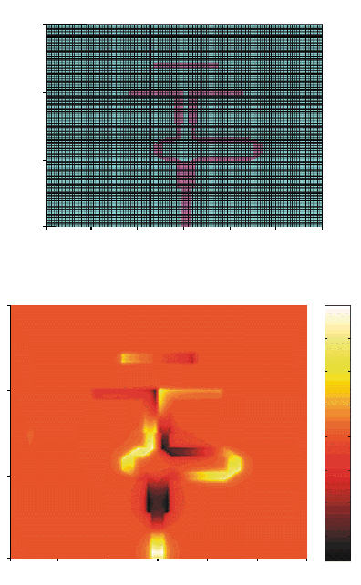
  This transition is inherently broadband.14 In addition, a periodic structure of transverse slots is used to suppress excitation of the fundamental even mode. Figure 9 shows the cross section of the antenna's electric field profile with and without the mode suppressor. In the top figure, a substantial amount of asymmetry in the vertical field can be observed, indicating that both the fundamental (even) and the leaky
 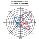 (odd) modes are present. In the bottom figure, the mode purity is improved significantly as indicated by the field null that has been shifted to the center of the microstrip. The antenna demonstrated a measured bandwidth of 20.2 percent.15 Simulated and measured radiation patterns of the structure are shown in Figure 10 . Note that both simulation and measurement indicate a substantial (-9 dB) lobe at -35°. This characteristic is a result of substantial power being reflected from the open end of the 5-l-long antenna. Simulation of a 10-l-long version indicates that the lobe will be reduced to -13 dB.
Tapered Slot Antennas
In the last decade, quite a bit of work has been conducted on tapered slot antennas (TSA) on dielectric substrates.16-17 These systems are completely planar, have an endfire pattern and are capable of obtaining high directivity and/or bandwidth. Proposed applications include millimeter-wave imaging, power combining and use as an active integrated antenna element. The TSA is etched into the metallization on one side of a dielectric substrate. The dielectric constant is usually low. Three popular configurations are shown in Figure 11 : the Vivaldi (exponential taper), linear TSA (LTSA) and constant-width slot antennas (CWSA). Radiation of a particular frequency occurs where the slot is a certain diameter. Slot width should reach at least one-half wavelength for efficient radiation to occur. Therefore, maximum and minimum widths roughly determine the bandwidth of the structure.
TSAs are usually built on thin, low permittivity substrates if they are to achieve good radiation patterns and maintain good radiation efficiency, which will be reduced by TM0 surface-wave losses. As with the patch antenna, micromachining has been used to reduce the electrical thickness of millimeter-wave TSAs by reducing the effective permittivity.3 This construction also allows a physically thicker substrate, which is essential for mechanical support for this kind of structure at millimeter wavelengths.
 Additionally, when used as an integrated antenna, a transition from the transmission line of choice (typically, microstrip or CPW) must be used. The bandwidth of the transition may limit the bandwidth of the structure. A CPW-fed TSA slot with exponential taper is shown
 in Figure 12 . The antenna is fabricated on a 25-mil substrate with 10.2 permittivity. The broadband CPW-slotline transition allows broadband response; measured bandwidth is greater than 70 percent centered at 13 GHz,18 as shown in Figure 13 .
Printed Quasi-Yagi Antennas
Printed wire antennas are planar adaptations of wire antennas such as the dipole, loop or spiral antenna. Only limited success has been achieved with developing working versions of truly planar wire antennas, due in part to the popularity of microstrip and coplanar waveguide transmission lines at these frequencies, which are difficult to integrate with wire-based antennas. For instance, a printed microstrip dipole has a very small radiation resistance due to the shorting effect of the microstrip ground plane and, consequently, will have low efficiency when realistic estimates of losses are made. This deficiency can be overcome by using an electrically thick substrate (at the cost of increased losses due to substrate waves and increased weight and cost).
Alternatively, the microstrip ground plane can be modified to accommodate the printed wire antenna. Recently, a new type of microstrip-compatible planar endfire antenna based on the well-known Yagi-Uda antenna has been discussed.19-21 The classic Yagi-Uda antenna consists of a driven element, reflector and one or more directors. The reflector and directors act as parasitic elements. The antenna has an endfire pattern and demonstrates high gain, but typically has a narrow bandwidth.
 The new architecture and an X-band prototype quasi-Yagi antenna are shown in Figures 14 and 15 , respectively. The antenna uses the truncated microstrip ground plane as the reflector and a microstrip-CPS transition as a balanced feed on a single-layer high dielectric substrate (Duroid, er = 10.2).14 The odd excitation of the CPS-driven dipole is clearly evident in the FDTD simulation of the current distribution, shown in Figure 16 . The X-band antenna uses 0.635-mm-thick Duroid.
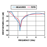
 The antenna radiates an endfire beam with a front-to-back ratio greater than 15 dB and cross-polarization level below -12 dB across the entire frequency band. A very low mutual coupling level below -22 dB has been measured for a two-element array with l/2
 separation. A plot of both FDTD simulation and measurement results for the input return loss is shown in Figure 17 . The simulated and measured bandwidths (SWR < 2) are 43 and 48 percent, respectively, which cover the entire X-band. The antenna is at least two orders smaller in volume than a standard horn antenna for the same frequency coverage. Radiation patterns of the endfire antenna are shown in Figure 18 .
It was also determined that the quasi-Yagi antenna can be scaled linearly to any frequency band of interest while retaining its wideband characteristics. In fact, a C-band prototype simulated and fabricated on 1.27-mm-thick Duroid (er = 10.2) measured 50 percent frequency bandwidth (4.17 to 6.94 GHz). FDTD simulation for a millimeter-wave version indicates that a single quasi-Yagi antenna works from 41.6 to 70.1 GHz (51 percent bandwidth), which covers part of the Q- and most of the V-band.
This antenna should prove to be a good array element and find application in any architecture that has been proposed for TSAs, such as imaging arrays and power combining. The antenna has several additional advantages over the tapered slot, including narrower width, direct microstrip feeding and the ability to be designed on a high permittivity substrate. Additionally, radiation efficiency may be improved because of the truncated ground plane, eliminating losses due to TM0 mode in the antenna region that may be a significant loss mechanism with the TSA.
Antenna Selection
The antennas presented in this article were chosen either for their novelty or for demonstration of fundamental concepts in planar antenna design and by no means represent all classes of planar antennas. For the sake of convenience, Table 1 lists a planar antenna selection chart that summarizes the characteristics of the antennas presented as well as a few other types of planar antennas that have been used at microwave and millimeter-wave frequencies. While still far from complete due to the vast amount of excellent research performed in this area, this article was intended to provide a flavor of what is possible with planar antennas as well as some additional insight.
|
Table I | |||||
|
Antenna |
Pattern |
Directivity |
Polarization |
Bandwidth |
Comments |
|
Patch |
broadside |
medium |
linear/circular |
narrow |
easiest design |
|
Slot |
broadside |
low/medium |
linear |
medium |
bidirectional |
|
Ring |
broadside |
medium |
linear/circular |
narrow |
feeding complicated |
|
Spiral |
broadside |
medium |
linear/circular |
wide |
balun and absorber |
|
Bow-tie |
broadside |
medium |
linear |
wide |
same as spiral |
|
TSA (Vivaldi) |
endfire |
medium/high |
linear |
wide |
feed transition |
|
Yagi slot |
endfire |
medium |
linear |
medium |
two-layer design |
|
Quasi-Yagi |
endfire |
medium/high |
linear |
wide |
uniplanar, compact |
|
LPDA |
endfire |
medium |
linear |
wide |
balun, two layer |
|
Leaky Wave |
scannable |
high |
linear |
medium |
beam-stearing, beam tilting |
Conclusion
A variety of planar antennas have been discussed. Resonant-type antennas, such as the patch and slot, are low profile and compact and can be readily integrated into large, active arrays. The antennas' broad patterns also make them useful in mobile handsets. Other more exotic planar antennas, such as the microstrip leaky wave, demonstrate higher directivity and the ability for frequency scanning. The quasi-Yagi antenna demonstrates the surprising amount of functionality that can be achieved with planar antennas. Its compact size, broad bandwidth and good patterns provide a viable alternative to antennas based on other technologies. As planar antenna technology continues to mature, the functionality of these antennas is expected to increase and drive penetration of commercial wireless communications to even higher frequency applications.
Acknowledgment
This work was supported by ONR MURI N00014-97-1-0508 and Sony MICRO. The authors wish to thank the student researchers at UCLA who contributed much of the data, including Ben Chang, Kuang-Ping Ma, Noriaki Kaneda and Phil Yang.
References
1. V. Radisic, Y. Qian and T. Itoh, "Novel Architectures for High Efficiency Amplifiers for Wireless Applications," IEEE Transactions on Microwave Theory and Techniques, Vol. 46, No. 11, November 1998.
2. D.M. Pozar, "Microstrip Antennas," Proceedings of the IEEE, Vol. 80, No. 1, January 1992.
3. G.M. Rebeiz, "Millimeter-wave and Terahertz Integrated Circuit Antennas," Proceedings of the IEEE, Vol. 80, No. 11, November 1992.
4. G.P. Gauthier, A.C. Courtay and G.M. Rebeiz, "Microstrip Antennas on Synthesized Low Dielectric-constant Substrates," IEEE Transactions on Antennas and Propagation, Vol. 45, No. 8, August 1997.
5. Y. Qian, R. Coccioli, D. Sievenpiper, V. Radisic, E. Yablonovitch and T. Itoh, "A Microstrip Patch Antenna Using Novel Photonic Band-gap Structures," Microwave Journal, Vol. 42, No. 1, January 1999, pp. 66-76.
6. H.G. Booker, "Slot Aerials and Their Relation to Complementary Wire Aerials," Journal IEE (London), Part IIIA, Vol. 93, 1946, pp. 620-626.
7. Yoshikazu Yoshimuar, "A Microstripline Slot Antenna," IEEE Transactions on Microwave Theory and Techniques, November 1972.
8. Thomas M. Weller, Linda P.B. Katehi and Gabriel M. Rebeiz, "Single and Double Folded-slot Antennas on Semi-infinite Substrates," IEEE Transactions on Antennas and Propagation, Vol. 53, No. 12, December 1995, pp. 1423-1428.
9. H.S. Tsai, M.J.W. Rodwell and R.A. York, "Planar Amplifier Array with Improved Bandwidth Using Folded Slots," IEEE Microwave and Guided Wave Letters, Vol. 4, No. 4, April 1994.
10. W.R. Deal, V. Radisic, Y. Qian and T. Itoh, "A Broadband Microstrip-fed Slot Antenna," 1999 IEEE MTT-S Topical Symposium Digest, pp. 202-212.
11. T.L. Chen and Y.D. Lin, "Aperture-coupled Microstrip Line Leaky-wave Antenna with Broadside Main Beam," Electronic Letters, Vol. 34, No. 14, July 1998.
12. Y.D. Lin, J.W. Sheen and C.K.C. Tzuang, "Analysis and Design of Feeding Structures for Microstrip Leaky-wave Antenna," IEEE Transactions on Microwave Theory and Techniques, Vol. 44, No. 9, Sept.1996.
13. Y.D. Lin and J.W. Sheen, "Mode Distinction and Radiation-efficiency Analysis of Planar Leaky-wave Line Sources," IEEE Transactions on Microwave Theory and Techniques, Vol. 45, No. 10, October 1997.
14. Y. Qian and T. Itoh, "A Broadband Uniplanar Microstrip-to-CPS Transition," 1997 Asia-Pacific Microwave Conference Digest, December 1997, pp. 609-612.
15. Y. Qian, B.C.C. Chang, T. Itoh, K.C. Chen and C.K.C. Tzuang, "High Efficiency and Broadband Excitation of Leaky Mode in Microstrip Structures," presented at the 1999 IEEE MTT-S, Anaheim, CA.
16. K.S. Yngvesson, D.H. Schaubert, T.L. Korzeniowski, E.L. Kollerg, T. Thungren and J.F. Johansson, "Endfire Tapered Slot Antennas on Dielectric Substrates," IEEE Transactions on Antennas and Propagation, Vol. 33, No. 12, December 1985.
17. K.S. Yngvesson, T.L. Korzeniowski, Y.K. Kim, E.L. Kollberg and J.F. Johansson, "The Tapered Slot Antenna - A New Integrated Element for Millimeter-wave Applications," IEEE Transactions on Microwave Theory and Techniques, Vol. 37, No. 2, February 1989.
18. K.P. Ma, Y. Qian and T. Itoh, "Analysis and Application of a New CPW-slotline Transition," IEEE Transactions on Microwave Theory and Techniques, Vol. 47, No. 4, April 1999.
19. N. Kaneda, Y. Qian and T. Itoh, "A Novel Yagi-Uda Dipole Array Fed by a Microstrip-to-CPS Transition," Aisa-Pacific Microwaves Conference Digest, 1998.
20. Y. Qian, W.R. Deal, N. Kaneda and T. Itoh, "Microstrip-fed Quasi-Yagi Antenna with Broadband Characteristics," Electronic Letters, Vol. 34, No. 23, November 1998.
21. Y. Qian, W.R. Deal, N. Kaneda and T. Itoh, "A Uniplanar Quasi-Yagi Antenna with Wide Bandwidth and Low Mutual Coupling Characteristics," to be presented at the 1999 AP-S, Orlando, FL.