
Characterization of a Double-doped Power HJFET for W-CDMA Cellular Handset Application
Demands on next-generation wideband CDMA (W-CDMA) handset transmitters (and thus power devices) include high linearity and high power-added efficiency (PAE) under low voltage supply. A power heterojunction FET (HJFET) has been developed for such applications, achieving a high PAE of 44.2 percent with a first adjacent-channel leakage power ratio (ACPR1) of -43 dBc at an output power of 28 dBm. This article illustrates the optimum device structure with emphasis on achieving low device on resistance suitable for low voltage operation. The importance of selecting proper source and load impedances and quiescent drain current level for the HJFET is detailed, with particular focus on attaining high PAE and low ACPR1 under the W-CDMA standard.
G. Hau, T.B. Nishimura and N. Iwata
NEC Corp., Kansai Electronics Research Laboratories
Shiga, Japan
Cellular communication has experienced rapid growth in recent years. Emerging requirements for multimedia access and the continuous demands for higher system capacity and better spectrum efficiency have driven the development of the third-generation cellular standard (IMT-2000).
W-CDMA has emerged as one of the leading air interface solutions and currently is in its initial development stage.1-3 The W-CDMA system employs spectrally efficient, nonconstant envelope digital modulation schemes to improve spectrum efficiency. Together with the wide bandwidth definition, W-CDMA has placed a more stringent regulatory requirement on ACPRs than other current digital cellular standards, such as IS-95.4 Therefore, highly linear transmitters are demanded for W-CDMA handset applications.
The characterization of handset transmitters is usually dominated by the power devices used. Therefore, selecting the appropriate device is vital for optimum operation. Although a variety of device technologies are available for power application, it has been demonstrated that HJFET is a leading candidate for W-CDMA handset transmitter applications due to its high PAE and low ACPR characteristics.5-7 The high PAE is achieved by biasing the HJFET with a very low quiescent drain current Iq instead of a higher Iq (class A operation); W-CDMA ACPR requirements are satisfied under this operation, attributed to an ACPR dip phenomenon.
In this article, an extensive study on the characteristics of a double-doped power HJFET developed for W-CDMA cellular telephones is presented. The optimum device structure is first illustrated with emphasis on achieving low device on resistance Ron suitable for low voltage operation. The effects of source and load impedances and quiescent drain current level on the HJFET's performance are detailed, with particular focus on attaining high PAE operation according to the W-CDMA standard. Two distinct ACPR characteristics due to different Iq operations are addressed and their dependence on optimum load impedances are discussed. The correlation between ACPRs and third- and fifth-order intermodulation (IM3 and IM5, respectively) distortions are examined. Based on the close correlation, a first-channel ACPR dip phenomenon is explained in terms of a similar IM3 characteristic.
Device Structure and DC Characteristics
 The characteristics of power devices usually dominate the performance of handset transmitters. To achieve the goals of high efficiency under low voltage operation, an optimum device structure with low Ron is indispensable.8,9 Figure 1 shows the optimized structure of the developed double-doped AlGaAs/InGaAs/AlGaAs HJFET. A multilayer cap structure was employed to reduce the Ron of the HJFET.6 A double-recess structure, fabricated by electron cyclotron resonance plasma dry-etching,10 was adopted to suppress parallel conduction and surface trapping effects, which further reduce Ron and prevent premature power saturation.11 With this optimized structure, the HJFET demonstrates a low Ron of 1.4 W-mm. The active part of the HJFET consists of a 15-nm-thick undoped In0.2Ga0.8As channel layer sandwiched between upper and lower Si-doped Al0.22Ga0.78As donor layers. A 15-nm-thick undoped Al0.22 Ga0.78As Schottky layer was incorporated on the upper Si-doped Al0.22 Ga0.78As layer to achieve a high gate-to-drain breakdown voltage BVgd.11 WSi metal was sputter deposited onto the narrow recess to form a 0.7-mm-long gate.
Figure 2 shows the drain I-V characteristics of the HJFET. The fabricated HJFET exhibited a maximum drain current Imax of 580 mA/mm at a gate-to-source voltage Vgs of 1.25 V. A maximum transconductance gm of 400 mS/mm was achieved at Vgs = 0 V. The BVgd was 14.2 V, measured at a gate current density of 1 mA/mm, and the threshold voltage was -0.6 V.
HJFET Power Performance
Characteristics of power devices such as output power level, linearity and PAE are related to the source and load terminations. In addition, biasing current also plays a critical role in determining device characteristics.5,6 To obtain the optimum device performance, these parameters must be properly chosen. The effect of these parameters on the W-CDMA performance of the developed HJFET is investigated.
 The W-CDMA characteristics of the double-doped HJFET with a gate width of 24.6 mm were evaluated using a QPSK modulated signal with a chip rate of 4.096 Mcps at 1.95 GHz under various Iq conditions. The optimum source and load impedances were determined through source/load-pull measurement to obtain a maximum PAE while maintaining an ACPR1 (defined at 5 MHz offset from the carrier frequency with a bandwidth of 4.096 MHz) of less than -43 dBc and an output power Pout of 28 dBm. The measured performance of the HJFET is shown in Figure 3 with an Iq of 80 mA (less than one percent of the maximum drain current Imax). At a drain bias voltage Vds of 3.5 V, the HJFET exhibited a PAE of 44.2 percent with a Pout of 28 dBm and an ACPR1 of -43 dBc. An ACPR1 dip is observed as a function of input power Pin at approximately 16 dBm. The dip behavior was determined to be important for the HJFET to achieve high PAE within the W-CDMA criteria.
The characteristic of the same HJFET was also measured under a higher Iq level of 300 mA (three percent of Imax) with the same source and load conditions. The measured result is shown in Figure 4 . The HJFET exhibited a lower PAE of 33.2 percent with Pout and ACPR1 levels similar to the lower Iq case. The ACPR1 only increases monotonically with the input power and no dip characteristic is observed.
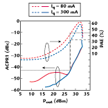 Figure 5 shows a comparison of the ACPR1 and PAE of the HJFET as functions of Pout for Iq = 80 and 300 mA. Both operations achieve the -43 dBc ACPR1 requirement at Pout = 28 dBm, but the higher Iq operation (300 mA) offers a better ACPR1 for Pout below 26 dBm. It can be seen that the linearity of the HJFET is improved due to the ACPR1 dip phenomenon under the low Iq condition at Pout of approximately 28 dBm. As a result of the dip, ACPR1 satisfies the specification resulting in a significant improvement in the PAE over higher Iq operation.
 The effect of load match on the HJFET PAE and W-CDMA ACPR1 characteristics was also investigated. The measured performance of the HJFET under three different load conditions is shown in Figures 6 and 7 for Iq = 80 and 300 mA, respectively. A compromise on the load match between maximum Pout and PAE must be chosen to
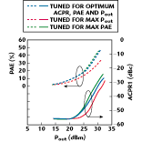 achieve the highest PAE and optimum ACPR1 at the required Pout level. A similar condition is observed for the higher Iq case. It is interesting to note that the ACPR1 dips occur under various cases of load match for the low Iq operation, whereas no such dip appears for the higher Iq case. The dip characteristic shown here thus can be exploited to improve the PAE of the HJFET while satisfying the ACPR1 specification provided the Iq level is appropriately chosen.
Correlation between W-CDMA ACPRs and IM Distortions
Linearity of devices is commonly expressed in terms of either ACPR or intermodulation distortion, depending on the nature of the system (digital or analog). Although ACPR and intermodulation distortion are two different measures, it has been shown that they could be correlated to each other to a certain extent in systems such as North American Digital Cellular and personal digital cellular.12 Here, the W-CDMA ACPRs of the developed HJFET are compared to its two-tone intermodulation characteristics.
 Figure 8 shows the ACPR definition of the W-CDMA system. The first and second adjacent channels are defined at 5 and 10 MHz offset from center frequency, respectively, with a bandwidth of 4.096 MHz. The first and second adjacent-channel ACPRs (ACPR1 and ACPR2, respectively) are defined as the ratio of the main channel power to the first and second adjacent-channel leakage power, respectively. The bandwidths of the IM3 and IM5 distortions are also shown and are estimated based on the bandwidth of the mixing frequencies. Both the IM3 and IM5 distortions fall within the first adjacent channels, whereas only the IM5 distortion is within the second adjacent channel.
The W-CDMA ACPRs of the HJFET were measured with a QPSK-modulated signal having a chip rate of 4.096 Mcps at 1.95 GHz; the intermodulation distortions were measured using a two-tone input signal at frequencies of 1.948 and 1.952 GHz. Figure 9 shows the ACPRs and intermodulation distortions of the HJFET under the low Iq operation (80 mA). ACPR1 closely follows the characteristic of the IM3 distortion with an offset value. The discrepancy at low input power is due to the limited dynamic range of the measurement system. The IM5 distortion is noted to have no obvious correlation with the ACPR1 characteristic, possibly due to its magnitude that is lower than that of the IM3 distortion. It can be clearly seen that the ACPR1 dip arises from a similar characteristic on the IM3 distortion near the same Pout level. For the ACPR2, it shows a good correlation to the IM5 distortion.
 Figure 10 shows the ACPRs and intermodulation distortions of the HJFET under a higher Iq level of 300 mA. Similar to the low Iq case, ACPR1 and ACPR2 are correlated to the IM3 and IM5 distortions, respectively. However, ACPR1 is distinctly different compared to the low Iq case. The ACPR1 dip does not occur and its level only increases with the output power.
 To further illustrate the correlation between W-CDMA ACPR1 and IM3 distortions, the load- and source-pull contours of the HJFET were
 measured. Figures 11 and 12 show the load- and source-pull ACPR1 and IM3 contours, respectively, plotted on a Smith chart (Z0 = 50 W) for an Iq = 300 mA. The input power was equal to 7 dBm in both cases. A good correlation between the ACPR1 and IM3 contours is seen in both figures.
Due to the close correlation, the ACPR1 dip is explained in terms of a similar  characteristic on the IM3 distortion. It is understood that the total distortion at IM3 frequency composes distortions generated by odd-order nonlinearities.13 Assuming the HJFET is weakly nonlinear (which would be valid under normal nonsaturation operation), its characteristic can be represented by up to the fifth-order nonlinearity. The overall distortion at IM3 frequency is therefore the vector sum of the distortions generated by the third- and fifth-order nonlinearities, as shown in Figure 13 . When the two distortions have a comparable magnitude and a near out-of-phase difference (q ª 180°), cancellation between these distortions would occur, resulting in a dip phenomenon.
A simulation was performed to verify the explanation. An HJFET model was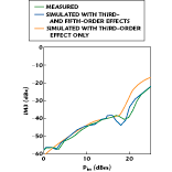 constructed using a large-signal equivalent circuit model, EEHEMT1, available in commercial microwave simulators.14 The two-tone characteristic was simulated using a harmonic balance technique, and good agreement between the measured and simulated results was observed. Figure 14 shows the simulated effect of third- and fifth-order nonlinearities of the HJFET on the overall IM3 level for the low Iq condition (80 mA). The harmonic contents and mixing order used in the simulation were chosen in a way that the two nonlinear effects could be separated. For example, the IM3 distortion generated by fifth-order nonlinearity can be eliminated with a mixing order of less than five. For the case with up to fifth-order nonlinearity, the simulated and measured results show good agreement. However, the IM3 dip does not occur when only the third-order nonlinearity is considered. For an input power below 10 dBm, the third-order nonlinearity dominates the overall IM3 level due to a more linear operation under small signal level.
 Figure 15 shows a comparison of the simulated amplitude and phase differences between the two distortions generated by the third- and fifth-order nonlinearities at the IM3 frequency for the low Iq operation. At an input power of approximately 16 dBm, the two distortions have a close amplitude response (near 0 dB amplitude difference) and their phase difference q is nearly 180°. These characteristics satisfy the conditions for signal cancellation discussed previously, resulting in the IM3 dip. However, these conditions are only limited to a certain output power level. The ACPR1 dip under the W-CDMA specification also can be explained in a similar manner due to its strong correlation with the IM3 distortion discussed previously.
Conclusion
A double-doped HJFET has been developed to operate at a 3.5 V drain bias voltage for W-CDMA handset applications. The HJFET employs multilayer cap and narrow recess structures, demonstrating a low Ron of 1.4 W-mm that is suitable for low voltage operation. Operating at a low Iq of 80 mA, the HJFET exhibited a high PAE of 44.2 percent and an ACPR1 of -43 dBc at an output power of 28 dBm, achieving significant PAE improvement compared to the high Iq operation. The high PAE achieved is attributed to the optimum device structure and specific source and load tunings as well as the ACPR1 dip under the low Iq condition. The results demonstrate that the developed HJFET is suitable for W-CDMA handset transmitter applications.
The correlation between W-CDMA ACPRs and HFET intermodulation distortions was discussed. It was shown that the W-CDMA ACPR1 and ACPR2 are strongly correlated to IM3 and IM5 distortions, respectively. The origin of the ACPR1 dip phenomenon was determined to be correlated to a similar characteristic on the IM3 distortion. The IM3 dip (and, therefore, the ACPR1 dip) is attributed the cancellation of distortions generated by the third- and fifth-order nonlinearities at the IM3 frequency.
Acknowledgment
The authors wish to thank M. Kuzuhara, I. Mito and M. Ogawa for their encouragement and support throughout this work.
References
1. NTT Mobile Communication Network Inc., W-CDMA, NTT DoCoMo Brochure, November 1997.
2. K. Hansen, "Wireless Communications Devices and Technology: Future Directions," IEEE Radio Frequency Integrated Circuits Symposium Digest, Baltimore, MD, June 1998, pp. 1-5.
3. R. Prasad and T. Ojanpera, "An Overview of CDMA Evolution toward Wideband CDMA," IEEE Comm. Surveys, Vol. 1, No. 1, 1998, pp. 2-29.
4. S. Brozovich, "Ultra Linear, High Efficiency Power Amplifiers: A Modern Paradox," IEEE MTT-S International Microwave Symposium Workshop Digest on Power Amplifier Design for Digital Wireless Systems, Denver, CO, June 1997.
5. T.B. Nishimura, N. Iwata, K. Yamaguchi, K. Takemura and Y. Miyasaka, "3.5 V Operation Driver-amplifier MMIC Utilizing SrTiO3 Capacitors for 1.95 GHz Wideband CDMA Cellular Telehones," IEEE MTT-S International Microwave Symposium Digest, Baltimore, MD, June 1998, pp. 447-450.
6. T.B. Nishimura, N. Iwata, M. Tomita and Y. Bito, "44 Percent Efficiency Power Heterojunction FET Operated at 3.5 V for 19.5 GHz Wideband CDMA Cellular Telephones," Topical Workshop on Heterostructure Microelectronics for Information Systems Applications Digest, Kanagawa, Japan, September 1998, pp. 32-33.
7. G. Hau, T.B. Nishimura and N. Iwata, "Distortion Analysis of a Power Heterojunction FET under Low Quiescent Drain Current for 3.5 V Wideband CDMA Cellular Telephones," IEEE MTT-S International Topical Symposium Technological Wireless Application Digest, Vancouver, Canada, February 1999, pp. 37-40.
8. P. Asbeck, J. Mink, T. Itoh and G. Haddad, "Device and Circuit Approaches for Next-generation Wireless Communications," Microwave Journal, Vol. 42, No. 3, February 1999, pp. 22-42.
9. M. Golio, "Low Voltage Electronics for Portable Wireless Applications: An Industrial Perspective," IEEE MTT-S International Microwave Symposium Digest, Baltimore, MD, June 1998, pp. 319-322.
10. H. Oikawa, M. Kohno, A. Mochizuki and Y. Nashimoto, "Low Damage and Selective Etching of GaAs Using BCL3/SF6 Gas in ECR Plasma," Electrochemical Society Proceedings, Vol. 96-2, 1996, pp. 246-252.
11. N. Iwata, K. Inosako and M. Kuzuhara, "3 V Operation L-band Power Double-doped Double Heterojunction FETs," IEEE MTT-S International Microwave Symposium Digest, Atlanta, GA, June 1993, pp. 1465-1468.
12. J.F. Sevic, M.B. Steer and A.M. Pavio, "Large-signal Automated Load-pull of Adjacent-channel Power for Digital Wireless Communication Systems," IEEE MTT-S International Microwave Symposium Digest, San Francisco, CA, June 1996, pp. 763-766.
13. S.A. Maas, Nonlinear Microwave Circuits, Artech House, Norwood, MA, 1988.
14. Microwave and RF Design Systems Designer's Task Reference, Hewlett-Packard Co., 1994.
Gary Hau received his BEng degree from the City University of Hong Kong, Hong Kong in 1992, and his MSc and PhD degrees from the University of Leeds, UK in 1993 and 1998, respectively, all in electronic engineering. He joined NEC Corp., Japan in 1998. His work involves research and development of MMIC power amplifiers and other RF components for W-CDMA cellular handsets. Hau's research interests include modeling and analysis of active devices, amplifier linearization techniques and low distortion, high efficiency MMIC power amplifier design.
Takeshi B. Nishimura received his BE and ME degrees in material engineering from Kyoto University and the University of Tokyo in 1991 and 1993 respectively. He joined NEC Corp. in 1993 and has been engaged in the research and development of microwave GaAs devices and MMICs. Nishimura is a member of the Institute of Electronics, Information and Communication Engineers and the Institute of Electrical and Electronics Engineers.
Naotaka Iwata received his BE degree in materials science from the University
of Electro-Communications in 1981, and his ME and PhD degrees in materials science from the University of Tsukuba in 1983 and 1999, respectively. He joined NEC Corp. in 1983 where he was engaged in the growth and characterization of III-V compound semiconductors. Since 1989, Iwata has been involved in the research and development of high power FETs using III-V compound semiconductor heterojunctions. He is a member of the Institute of Electronics, Information and Communication Engineers and the Institute of Electrical and Electronics Engineers.