
Electromagnetic (EM) simulation software is commonly used to simulate antennas with multiple feeds, including phased arrays, stacked radiators with different polarizations and single apertures with multiple feed points. These types of antennas are popular for communication systems where multiple-input-multiple-output (MIMO) and polarization diversity antenna configurations are being used. It is expected that their use will explode with the rollout of 5G wireless systems.
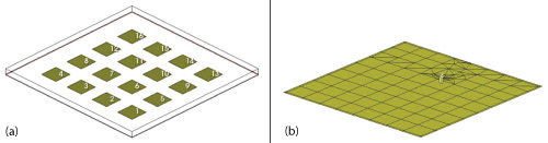
Figure 1 4 × 4 patch array (a). Single element mesh, with its driving pin to the ground plane (b).
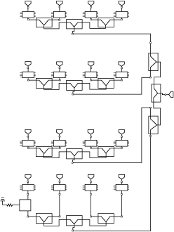
Figure 2 Patch array corporate feed network.
The antenna’s beam is controlled by changing the phase and amplitude of the signals going into the various feeds. The problem for simulation software is that the antenna and the driving feed network influence each other. The antenna’s pattern is changed by setting the input power and relative phasing of the signals at its various ports. At the same time, the input impedances at these ports change with the antenna pattern. Since input impedance affects the performance of the nonlinear driving circuit, the changing antenna pattern affects overall system performance.
Until now, engineers have had to simulate the coupled antenna/circuit effects manually using some sort of iterative process. For example, the antenna is first driven with idealized sources having known phasing at the input ports. The impedance of the ports is then used as the load impedance for the driving circuit. The process is iterated over and over until convergence is reached. This procedure is awkward at best. Fortunately, new in-situ technologies within RF/microwave design software now provide a more efficient and accurate way to reach the final result.
These new in-situ measurement features enable the circuit and antenna to talk to each other, thus automatically accounting for the coupling between the antenna and the circuit in an easy-to-use framework. The designer identifies the antenna data source, the circuit schematic driving the antenna and the measurement under consideration; for example, power radiated over scan angle. This concept is illustrated in the following phased-array example, where the antennas are simulated in a NI AWR Design Environment™ (inclusive of Microwave Office circuit design software, AXIEM 3D planar EM and Analyst™ 3D finite-element method (FEM) EM simulators).
Patch Microstrip Array Simulation Example
In this example a 4 × 4 patch array is simulated. It is driven by a corporate feed network with a phase shifter and attenuator at each element. A monolithic microwave integrated circuit (MMIC) power amplifier is placed at each element before its corresponding phase shifter. The array is simulated just once in the EM simulator. The resulting S-parameter file is then used by the circuit simulator, which includes the feed network and amplifiers. As the phase shifters are tuned over their values, the antenna’s beam is steered. At the same time, each amplifier sees the changing input impedance at the antenna input it is attached to; and this, in turn, affects the amplifier’s performance. The power amplifiers are nonlinear, designed to operate at their P1dB compression points for maximum efficiency. They are, therefore, sensitive to the changing load impedances presented by the array.
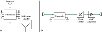
Figure 3 Wilkinson divider and transmit module (a), block diagram of the transmit module (b).
Combined circuit and EM simulations are necessary for a number of other reasons. First, antenna element interaction can degrade antenna performance. An extreme example is scan blindness, where element interaction causes no radiation to occur at certain scan angles. Coupling between elements can also lead to feed network resonances. In order to optimize the feed network to account for deficiencies in the antenna, the entire array and circuit, combined, must be optimized. It is also necessary to simulate the feed network, itself, as resonances can build up within it by the loading of the ports.
Important, though often not performed, is nonlinear circuit simulation of the power amplifier that drives the antenna. For this, the antenna’s S-parameters must include a DC simulation point, and values at the various harmonics used in the harmonic balance simulation. Otherwise, system performance degradation is possible due to poor matching at harmonic frequencies.
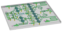
Figure 4 MMIC amplifier.
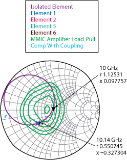
Figure 5 Circuit simulation results.
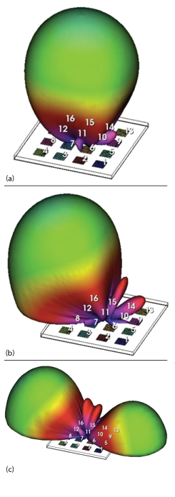
Figure 6 pical values of theta and phi. Broadside excitation (a), beam at θ = 30° and ϕ = 0° (b), beam at θ = 75° and ϕ = 0° (c).
Figure 1 shows the 4 × 4 patch antenna array. Each patch is fed individually by a pin to the ground below. The port is placed at the bottom of the pin. A 3D planar EM simulator is ideal for planar patch arrays since the patch is not in a package, and radiation effects are therefore included automatically. It should be noted that the simulation techniques described in this article do not depend on a specific EM simulator. For this example, antennas are simulated using Analyst, which is a 3D finite element (FEM) EM software application.
The corporate feed network is shown in Figure 2. Each element is driven by a MMIC amplifier, and controlled by a phase shifter and attenuator. RF power is input from the right side. Wilkinson dividers are used to split the signal and feed the sixteen patches. Figure 3 shows the feed for a typical patch. The transmit module is shown in detail in Figure 3b. Each transmit module has a phase shifter, attenuator and MMIC amplifier. The beam is steered by setting the phase and attenuation at the input to the MMIC amplifier and then routing the resulting signal to the patch. Phase and attenuation are controlled by variables in the software, which can be tuned and optimized as desired. In this manner, the beam is scanned.
Figure 4 shows a 3D view of the MMIC amplifier. It is a two-stage, eight-FET amplifier, designed to work in X-Band. In this example, the entire feed network is simulated by the circuit simulator. A more realistic example would simulate the layout of the feed network in an EM simulator to make sure the models are accurate and there is no unintended coupling between sections of the network.
Simulation Results
Typical circuit simulation results are shown in Figure 5. The Smith chart shows the input impedance to an isolated element and to elements when the entire array is simulated. Load-pull contours for power delivered to the load are also shown. The system is designed to work at 10 GHz. The purple curve shows the input impedance for an isolated patch from 6 to 14 GHz on a 50 ohm normalized Smith chart. The marker shows the normalized impedance at 10 GHz. The four crosses show the input impedances of four typical elements at 10 GHz. Note that the interaction between the elements in the array shifts the input impedance of each element relative to that of an isolated patch. The green contours are load-pull simulations for the MMIC amplifier, showing the power delivered to a load. The shifting of the impedances of the antenna feed results in a 0.5 dB degradation of power to the elements. (The power contours are in 0.5 dB increments.)
Examples of the antenna pattern are shown in Figure 6. The beam is steered by controlling the relative phase and attenuation to the transmit modules. In practice, the harmonic balance takes substantial time to run with 16 power amplifiers; therefore, the beam is steered with the amplifiers turned off. The designer then turns on the power amplifiers for specific points of interest. Note Figure 6c shows a second lobe created when the main lobe is at a near grazing angle.
In Figure 7, the antenna pattern is optimized for a specific scan angle. This example is for an 8 × 8 patch array. For simplicity, the amplifiers are not included in the optimization. Before completing the design, the amplifiers are turned on to determine their effect on performance. The plot is of total power in the beam, scanning in the theta direction with phi at zero degrees. The blue bars show the optimizer goals. The purple pattern is the original broadside pattern. The optimizer changes the phase and attenuation at the feeds to the patches. The resulting blue curve meets the goals for the main beam with acceptable sidelobe levels.
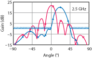
Figure 7 Antenna pattern optimized for gain above 20 dB at a 20° scan angle and with sidelobes below 0 dB at angles below 0° and above 45°.
Conclusion
In today’s complex communication systems utilizing antennas with multiple feed points, the interaction between the circuit (typically including a highly nonlinear power amplifier), the feed network and the antenna must be accounted for.The beam is steered by the circuitry, and as the beam changes the input impedance of the antenna changes, which affects the circuit. The antenna and the circuit are connected, so both must be included in the simulation.
The traditional method of simulating antennas with multiple feeds is to simulate coupled antenna/circuit effects manually, using an iterative process that is time consuming and frustrating. Modern RF/microwave design software couples the circuit and antenna simulation together. The load impedances of the array are incorporated into the circuit simulation. This automates the process, saving design time and delivering products to market faster