
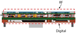
Figure 1 A receiver module with integrated RF and digital subsystems. The module is 3.25" × 0.5" × 1.4" and dissipates 27 W in the RF section and 22 W in the digital section.
With the continued drive to smaller form factor, such as smaller munitions and unmanned systems, the defense world is pushing the boundaries of electronic system integration and processing densities. Although smaller and smaller footprints are now becoming a reality, the challenge of thermal dissipation is often not considered. Yet meeting the thermal challenges, to ensure long term reliability and repeatable system performance, is becoming a more significant part of the system design, particularly considering the extreme temperature ranges over which many aerospace and defense systems must operate. To meet system size, weight and power (SWaP) needs, an increasing proportion of system design time needs to be allocated to the thermal challenges.
Consider a typical RF receiver and transmitter (see Figure 1), which could be the basis for a military radio, element digitization for a radar system or a communications link for an UAV or advanced munition. Depending on the frequency of operation and specific application, the system requires the integration of a number of functions and technologies to achieve optimum performance. The RF front-end requires power and low noise amplifiers, most likely based on GaAs or GaN. The mixing stages, intermediate amplifiers and synthesizers will be developed using GaAs or SiGe, with the digitizers and FPGA nodes on CMOS. This may result in four or five different technologies across the signal chain, with many more variations of process geometries. Integrating these can result in the need to dissipate 50 W or more in a few square inches and limited thermal pathways. GaN-based power amplifiers (PA), widely used in radar and electronic warfare (EW) systems, present other challenges with their system requirements and power density. For example, the PA shown in Figure 2 integrates two GaN MMICs, each dissipating 80 W. Multiple PAs are grouped close together to increase overall power.
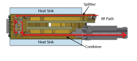
Figure 2 Cross-section of a power amplifier combining dual, 80 W GaN MMICs.
To optimize SWaP and cost, a thorough understanding of the thermal design is necessary to keep the temperatures of critical components within their operating bounds. Each technology and application has its own challenges from a thermal perspective, and the drive to reduced SWaP concentrates heat densities. The dissipation needs to be reviewed from multiple perspectives, as heat generated in the channel of a MMIC flows in a continuous chain through numerous layers and interfaces until it ultimately reaches the ambient environment. The entire chain must be reviewed to optimize system thermal performance, SWaP and cost.
Although the focus on system size reduction is certainly making the thermal challenge more complex, some relief is available from advanced process nodes and increasing device integration. Advanced SiGe and CMOS nodes are enabling significant power reduction, and increasing integrated digital signal processing is increasing integration. This supports increased functionality, often at power parity with previous generation architectures. The higher operating junction temperature of GaN reduces the cooling requirements for these individual components. However, process node migration is not enough to meet the thermal challenges. System miniaturization is seemingly moving faster.
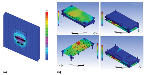
Figure 3 Die (a) and board (b) thermal simulations.
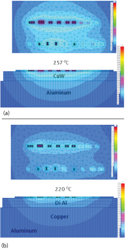
Figure 4 Thermal performance of 60 W GaN die attached to CuW and Al (a) vs. diamond-aluminum matrix on Cu and Al (b).
Simulation is Key
While building and testing prototypes continues to be critical in confirming design assumptions, the development times and high costs preclude efficient optimization based on hardware testing. Detailed simulation is essential and enables the rapid evaluation of multiple system variations. Trade-offs need to be evaluated from the entire system perspective. Multiple model levels and tools are required, as the geometry can scale six orders of magnitude, from sub-micron gates to meter-long housings. Heat generating and transfer mechanisms can include conduction, convection, radiation and EM energy. Simulation enables fast performance and cost trade-offs, optimizing from the device gate to system-level component placement, part design and material selection, as well as fan and heat sink specification (see Figure 3).
The maximum freedom comes from system designers who have control over the entire system chain, from the MMIC gate to the ambient environment. This allows a comprehensive approach to the thermal challenges, enabling trade-offs that may change device location and require device modifications. Accomplishing this often requires multiple models and software packages. Specialized analysis techniques such as computational fluid dynamics (CFD) for convection to fluids/air and electromagnetic simulations for RF losses can be used, with a handoff between each. For example, a rack mounted, air cooled, high power, solid-state amplifier used in radar or EW systems may need the following:
- Finite element analysis (FEA) with micron-scale meshing, including die level and heat spreader analysis
- Electromagnetic loss analysis to determine the power generated in RF lines
- FEA at the chassis level
- CFD analysis for airflow and convection to the ambient environment.
The greatest temperature deltas will typically occur at the locations of greatest heat concentration, which are ultimately near the gates. Typically, 70 percent of the temperature rise from ambient to junction is within the MMIC. With GaN power densities in radar systems now above 6 W/mm in some cases, simulating the trade-offs is critical.
Selecting the Right Materials
The choice and use of very high thermal conductivity materials to spread the heat are obviously critical. For example, with high power GaN die that are used in the latest PAs for radar, the substrate is typically SiC, and the first attach layer is AuSn solder. Over just 5 mils of material, the heat flux density may reduce from 13,000 W/mm2 to 24 W/mm2. As the heat continues to flow through the system, spreading will continue to reduce the flux density. The choice of materials is limited by matching the coefficient of thermal expansion (CTE), electrical conductivity to ground and the cost and ability to manipulate the material.
CTE mismatches can result in cracking of substrates or delamination of bonding layers, such as solder and epoxy. Cold storage and operating temperatures, critical aspects of aerospace and defense performance criteria, tend to cause the greatest CTE stresses, as the solders and epoxy are designed for processing at elevated temperature. Even mild delamination can have catastrophic effects on the thermal performance of a die, if the separation is in an area of high heat concentration — directly under a high power FET, for example. Comparing the hot spot temperatures on IR images of a design to known good images of the same design is a useful method for identifying early delamination when evaluating new materials.
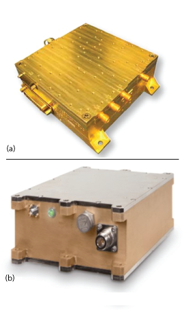
Figure 5 Examples of products using the integrated thermal design methodology: “man portable,” 5 W linear PA and up-converter (a) and 2 kW HPA (b).
Epoxy and sintered silver manufacturers are developing products with lower modulus of elasticity to absorb the CTE stresses while still retaining relatively good thermal performance. Heat conductivity close to the die is a key material research area, with extremely high thermal conductivity materials such as diamond being reviewed. As defense systems continue to look for reduced SWaP and cost, performance trade-off decisions for cost, weight and size are always intertwined in system architecture and thermal trade-offs. The use of materials such as diamond composites may seem hard to justify; however, using even small pieces of these materials as die heat spreaders in areas of high heat concentration can substantially reduce device temperatures and enable cost and weight savings in other parts of the system. Figure 4 compares two thermal simulations: a 60 W GaN die attached to a CuW carrier on an aluminum base vs. a diamond-aluminum matrix material carrier on a copper insert in an aluminum base. The latter reduced the junction temperature by some 37°C, providing improved system performance and life, while enabling other SWaP and cost tradeoffs elsewhere in the system.
In other examples, convection cooled systems, such as rack mounted, can be challenged with large temperature differences across the heat sink base and from the heat sink fins to the ambient air. Heat sink and fan choices have significant cost and performance impact and must be specified from a system perspective. For a given heat sink volume, better performance is driven by a higher convective heat transfer rate that requires greater back pressure, such as from tighter channels or staggered/slotted fins that break up boundary layers. This, in turn, requires larger and more power-hungry fans. The fan choice also impacts performance. Axial fans are typically the easiest to design with, providing high volume for low pressure systems, while centrifugal fans or blowers are able to push against higher pressure but with lower volume.
Lastly, the choice of heat sink material can significantly impact cost. In many cases, skived copper heat sinks seem to provide a good balance between performance and cost. Embedded heat pipes are also excellent low weight devices for enhancing the effective thermal conductivity of heat sink baseplates, although they do not work in all environments. High g-force environments pose a particular issue.
PUTTING IT ALL TOGETHER
Although it may seem that the thermal challenges are ominous, with many trade-offs, using a systematic approach can achieve solutions that balance cost, size and performance. Advanced simulations provide the backbone for quick decisions, enabling detailed analysis from the gate in the die to the system, as well as the impact of the heat sinks and heat spreaders. These advanced simulations help with trade-offs, from materials choices to cooling techniques and optimal layout. Applying these techniques with appropriate design decisions can yield systems with high heat concentration. Figure 5 shows two examples: a 37 W linear PA with integrated up-converter and a 2 kW solid-state high power amplifier (HPA). Both product designs utilized detailed simulation, which led to careful component integration, layout and material selection to balance performance and cost. The up-converter was designed to be “man portable,” so minimizing size and weight was an important requirement. Having the system and MMIC designed by the same team helped in balancing reliability, cost and performance.