
The increasing demand for wider bandwidth radar for finer range resolution to measure surface elevation and snow thickness over sea ice drives the need for ultra-wide bandwidth (UWB) receiver design. This article summarizes the design process for integrating and miniaturizing an UWB multichannel receiver, including receiver subsystem integration, co-simulation as well as the mechanical configuration.
At the University of Kansas Center for Remote Sensing of Ice Sheets (CReSIS), two UWB microwave radars have been developed and deployed to measure surface elevation and snow thickness over sea ice.1 The 2 to 8 GHz Snow Radar is used for measuring snow over sea ice, while a 12 to 18 GHz Ku-Band altimeter is used for high-precision surface elevation measurements.2 The systems have been deployed several times over the last decade on NSF and NASA platforms in conjunction with Operation Ice Bridge (OIB). In order to meet additional demands for snow characterization, a new multi-channel, quad-polarized 2 to 8 GHz Snow Radar has been developed with multi-polarization, multi-frequency and multi-look-angle capabilities. This article discusses the design approach and considerations for the multichannel receiver to comply with weight and size restrictions.
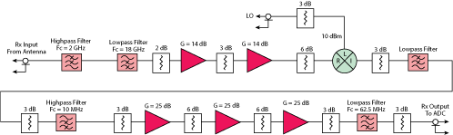
Figure 1 FMCW receiver block diagram.
Frequency Modulated Continuous Wave (FMCW) Receiver
FMCW radar is a form of continuous wave (CW) radar in which the frequency of the waveform is modulated. In most cases, this is linear modulation and the waveform is given the acronym LFMCW. This is commonly known as a chirp. A CW radar can detect only radial velocity using the Doppler Effect, while an FMCW radar can measure both radial velocity and range to the target.3
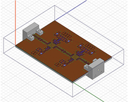
Figure 2 Integrated RF design in HFSS.
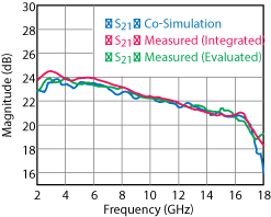
Figure 3 Receiver RF chain comparison.
Figure 1 shows a block diagram of the Snow Radar FMCW radar receiver. It consists of two subsystems: the radio frequency (RF) section and the intermediate frequency (IF) section. The RF section performs three tasks: filtering unwanted signals, setting the sensitivity of the receiver and mixing the return waveform with a reference waveform to produce an IF beat frequency.4 The IF section further filters out undesired signals while amplifying the desired beat frequency to fit within the dynamic range of the analog to digital converter (ADC).
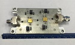
Figure 4 Integrated RF chain.
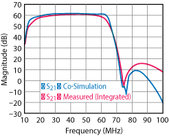
Figure 5 Receiver IF chain comparison.
RF Front-End Integration and Modeling
The first step in miniaturizing the receiver is to integrate the RF attenuators and amplifiers onto a single printed circuit board (PCB). Each component is characterized using a vector network analyzer (VNA) and then component S-parameter data is loaded into the Advanced Design System (ADS) as corresponding SXP files. A co-planar waveguide (CPWG) board topology is chosen due to its UWB and low loss performance. Initial simulation of the CPWG structure is performed in the Ansys High Frequency Structural Simulator (HFSS) where performance over the 2 to 18 GHz passband is optimized. After circuit board layout using the Easily Applicable Graphical Layout Editor (EAGLE), the design file is exported to HFSS for full board-level electromagnetic (EM) simulation.
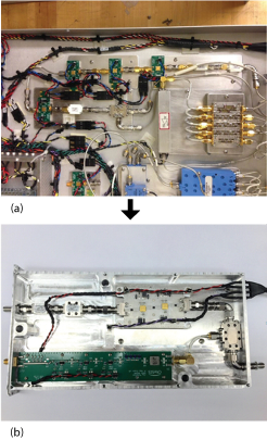
Figure 6 Original receiver (a) and new integrated receiver (b).
Figure 2 is a screen shot of the board in HFSS. Connectors are included in the design in order to appropriately taper the traces for matching. After running a full EM simulation, the S-parameters of the board are saved and loaded into ADS for co-simulation of the board and components. Co-simulated results and RF measurements of the original discrete component receiver and the integrated receiver board are in close agreement (see Figure 3). More importantly, measured performance of the integrated board over the passband agrees closely with that of the RF section in the original receiver. A significant size reduction is achieved without sacrificing RF performance.
The final version of the board is shown in Figure 4. It is fabricated on an LPKF mill and populated using a solder re-flow process. The board is epoxy bonded to a custom heat sink. Measurements are performed with a 10 MHz to 26.5 GHz Keysight N5222A VNA.
The benefit of this design process is that board performance is optimized and verified prior to fabrication, avoiding additional fabrication costs and schedule delays associated with a board re-spin.
IF Back-End Integration and Modeling
The same design procedure is used for the IF back-end. Individual IF components are characterized using the same VNA and the S-parameters are uploaded into ADS. The integrated IF board is laid out in EAGLE and then exported to HFSS for EM simulation. The board S-parameters are loaded into ADS to perform a full co-simulation. After minor adjustments, the board is fabricated, populated and tested. Figure 5 shows good agreement between simulation and measurement. Minor differences in the IF passband are due to the individual filter components used in the HFSS simulation. Because S-parameters for the capacitors used were not available, ideal lumped elements were substituted; therefore, cutoff frequencies and roll-offs are slightly degraded in the measured data.
Receiver Integration and Measurements
Figures 6a and 6b show the original receiver and the new integrated receiver, respectively. Integration of the RF and IF chains results in a size reduction of 5.5. The receiver employs a modular concept. The backplane has electromagnetic interference (EMI) filters passing power to the components and filtering unwanted signals coupled onto the twisted pairs. The mixer LO port protruding from the back allows a cable connection to supply LO drive power.
Measurements are made using the Keysight N522A VNA set up in mixer mode. The RF and LO ports are swept from 1 to 20 GHz with the IF frequency set to 40 MHz. The IF bandwidth is set to 5 kHz and the receivers are measured using 32,001 points. The cables used are calibrated for loss and subtracted from the receiver measurement in MATLAB. Figure 7 shows the response of the modular receiver. Gain variation across the 2 to 18 GHz passband is minimal. Components with low gain variation are used and fine-tuning of the RF board further minimizes variations. A highly selective DC to 18 GHz lowpass filter (LPF) and 2 GHz cutoff frequency highpass filter (HPF) define the passband and attenuate out-of-band signals.
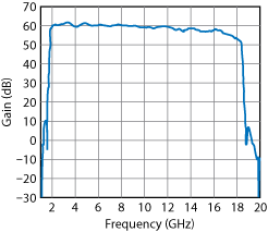
Figure 7 Measured receiver gain.
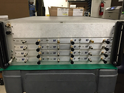
Figure 8 Front view of the receiver.
Mechanical Integration and Chassis Miniaturization
Enabled by the modular design of the individual receivers, the mechanical design accommodates multiple receivers inside a single chassis. A 4U Techmar case houses up to 18 individual receivers (see Figure 8). The photo shows 12 receiver units in their respective slots. The blank plate at the top of the chassis can be removed exposing six additional slots. The volume of the overall receiver chassis is reduced by a factor of 4 (for 18 channels) when compared to the original discrete component design.
All of the power supplies, power distribution boards and the LO distribution chain fit within the 4U mechanical case. Two power distribution boards bring a single voltage in and distribute it to all the receivers, a built-in feature that supports the modular design. The LO distribution is a chain of amplifiers and power splitters, allowing a single LO drive signal to be connected to the input of the receiver chassis. It is then split and amplified to satisfy mixer LO drive power requirements.
Conclusion
At the Center for Remote Sensing of Ice Sheets, UWB FMCW radars are used to accurately determine snow thickness. With increased demand for additional snow characterization to more accurately model polar climate change, a new multi-channel, quad-polarized, 2 to 18 GHz Snow radar has been developed. With a 5.5 times size reduction of the receiver, along with a modular design, an overall 4 times size reduction of the receiver chassis is accomplished. Elimination of long lead times and reduced cost is achieved by designing and developing the UWB filters in-house, along with other passive microwave components. Through size and weight reduction, UWB multichannel remote sensing is a plausible option to satisfy future research needs.
References
- D. Alvetegui, “ALinearization Method for a UWB VCO-Based Chirp Generator Using Dual Compensation,” Department of Electrical Engineering and Computer Science: Master’s Thesis, University of Kansas, 2011.
- F. Morales, S. Gogineni and C. Leuschen, “Advanced Multifrequency Radar Instrumentation for Polar Research,” IEEE Transactions on Geoscience and Remote Sensing,Vol. 52, No. 5, May 2014, pp. 2824–2842.
- M. I. Skolnik, “Introduction to RADAR Systems,” Third Edition, McGraw-Hill Book Co., 2002.
- M. Richards, J. Scheer and W. Holm, “Principles of Modern Radar,”SciTech Publishing, 2010.

Jay W. McDaniel received his B.S. degree in electrical engineering from Kansas State University in 2013, and is currently pursuing his M.S. degree in electrical engineering with an emphasis on applied electromagnetics at the University of Kansas. From 2013 to 2015, he worked as a Graduate Research Assistant at the Center for Remote Sensing of Ice Sheets (CReSIS) at the University of Kansas. His research interests include UWB FMCW radars for remote sensing and RF/microwave circuits and component design.

Jie-Bang Yan received his B.Eng. degree (first class honors) in electronic and communications engineering from the University of Hong Kong in 2006, his M.Phil. degree in electronic and computer engineering from the Hong Kong University of Science and Technology in 2008, and his Ph.D. in electrical and computer engineering from the University of Illinois at Urbana-Champaign in 2011. Upon graduation, he joined the Center for Remote Sensing of Ice Sheets (CReSIS) at the University of Kansas as an assistant research professor. His research interests include conformal and low-profile antennas and phased array designs for radar systems, ultrawideband phased arrays, antenna platform integration, design and analysis of MIMO and reconfigurable antennas, fabrication of on-chip antennas, RF propagation and radar remote sensing of the cryosphere.

Sivaprasad Gogineni received his B.E. degree from the University of Mysore, Mysore, India, in 1973, his M.Sc. degree from Kerala University, Thiruvananthapuram, India, in 1976, and his Ph.D. from the University of Kansas in 1984. He is currently a Deane Ackers Distinguished Professor with the electrical engineering and computer science departments at the University of Kansas, as well as the director of the National Science Foundation Science and Technology Center for Remote Sensing of Ice Sheets.