
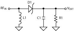
Figure 1 Schottky diode RF detector.
Because of their fundamental rectifying characteristic, diodes have been used to generate DC voltages that are proportional to AC and RF signal levels for as long as there have been diodes. This article compares the performance of diode-based RF/microwave detectors with integrated circuit alternatives. Topics include transfer function linearity, temperature stability and interfacing with analog-to-digital converters.
A popular diode RF detection circuit (see Figure 1) can be thought of as a simple half-wave rectifier with output filtering. The positive half cycles of the input signal forward bias the Schottky diode, which charges the capacitor. On the negative half cycle, the diode is reverse biased, causing the voltage on the capacitor to be held at a DC output that is proportional to the input signal. To allow this voltage to drop when the input signal decreases or is turned off, a resistor in parallel with the capacitor provides a discharge path. Figure 2 shows the transfer function of this circuit. The input power is scaled in dB, and the output voltage is plotted on a logarithmic scale.
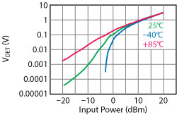
Figure 2 Transfer function of a Schottky diode RF detector.
The 25°C transfer function has two distinct operating regions on the curve. The so-called linear region extends from the top of the input range (approximately +20 dBm) down to around 0 dBm. This linear region derives its name because the output voltage is roughly proportional to the input voltage. Below 0 dBm, the so-called square law region begins, where the output voltage is roughly proportional to the square of the input voltage. The transfer function has a greater slope, as seen in the figure. Figure 2 also shows the output voltage vs. input power transfer functions when the temperature is between -40° and +85°C. These show significant deviations at power levels below 0 dBm, which renders the device unusable in applications where the temperature varies by any significant amount. Techniques can be used to mitigate this temperature drift somewhat. They involve introducing a second, reference diode that is either part of the circuit or a stand-alone circuit with its own output. The temperature drift of the reference diode matches that of the primary diode, so by a process of subtraction (either analog or digital, based on the circuit), some amount of drift can be cancelled.
Figure 3 shows the transfer function at 25 GHz of an integrated Schotky diode detector that has several novel features. As part of the signal processing, the input passes through a circuit which performs a “square rooting” function on signals below a certain power level. The transition point is set to equal the power level where the diode transitions from the square law to the linear region. As a result, the square law effect of the diode is cancelled, and there is no sign of the two-region transfer function that is so apparent in Figure 1. Figure 3 also shows the transfer function at various temperatures from -55°to +125°C, as well as the variation in the transfer function vs. temperature. Using linear regression of the 25°C transfer function as a reference, the error in dB is plotted at each temperature. With integrated temperature compensation and the square law elimination circuit, errors due to linearity and temperature drift are reduced to approximately ±0.5 dB over the majority of the input range.
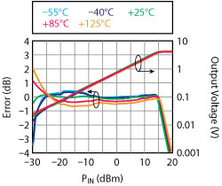
Figure 3 Improved performance of an integrated Schottky diode detector, measured at 25 GHz.
ADC INTERFACING
While RF/microwave detectors are sometimes used in analog power control loops, it is more common to build a digital power control loop (see Figure 4). In this configuration, the output of the power detector is digitized by an analog-to-digital converter (ADC). In the digital domain, the power level is calculated using the code from the ADC. Once the power level is known, the system will respond by adjusting the transmitted power if necessary. While the response time of this loop will depend to a small extent on the response time of the detector, the sampling rate of the ADC and the speed of the power control algorithm will have a far larger impact.
The loop’s ability to measure and precisely set the RF power level is impacted by several factors, including the transfer function of the RF detector and the resolution of the ADC. To illustrate, Figure 5 compares the responses of a diode detector and a microwave logarithmic amplifier (log amp), both at 20 GHz. The log amp has a transfer function that is linear in dB, where a 1 dB change in input power always results in the same voltage change at the output (over the linear input range from approximately -50 to 0 dBm). In contrast, the diode-based detector has a transfer function which appears exponential when plotting output voltage vs. input power in dB. Because ADCs have a transfer function that is scaled in bits per volt, system resolution in dB per bit continually decreases with decreasing input power. Figure 5 also shows the bits per dB resolution that would be achieved if the diode detector were to drive a 12-bit ADC with a full-scale voltage of 5 V (the plot is on a logarithmic secondary axis for ease of viewing). At the low end of the device’s power range, around -25 dBm, the incremental slope would be approximately 2 bits per dB, yielding a resolution of approximately 0.5 dB per bit. This suggests that a 12-bit ADC is adequate to accurately resolve the output of the diode detector IC over its full range. As the RF input power increases, the incremental slope in bits per dB increases steadily to a maximum of approximately 300 bits per dB at the maximum input power of +15 dBm. This is valuable in RF power control applications where accuracy is most critical when the system is at its maximum power. This is a very typical scenario in applications where RF detectors are used to measure and control the power of a high power amplifier (HPA). Where power is being controlled to prevent the HPA from overheating, high resolution power measurement at maximum power is very valuable. The transfer function of the log amp in Figure 5 has a constant slope over its linear operating range. This suggests that a lower resolution ADC (10-bit or possibly even 8-bit) would be adequate to achieve a resolution well below 1 dB.
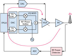
Figure 4 Typical digital RF power control loop.
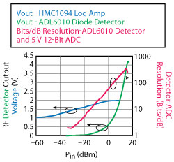
Figure 5 Performance comparison of integrated Schottky diode detector and log amp.
An application circuit where the diode detector interfaces with a 12-bit, 1 MSPS precision ADC is shown in Figure 6.The ADC has an internal 2.5 V reference which sets the full-scale input voltage. Because the diode detector can reach a maximum voltage of approximately 4.25 V, a simple resistive divider is used to scale this voltage so that it never exceeds 2.5 V. This scaling can be implemented without needing an op-amp buffer. The achievable resolution at the bottom of the input power range is similar to the example, i.e., approximately 0.5 dB per bit.
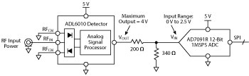
Figure 6 Application circuit for an integrated microwave power detector mated with a precision ADC.
Conclusion
Integrated RF/microwave detectors offer benefits when compared to discrete implementations. Integrated temperature compensation ensures the output voltage is stable to approximately ±0.5 dB over a wide temperature range. An internal square-rooting function effectively eliminates the square law characteristic at low input power, resulting in a single linear transfer function that simplifies device calibration. The buffered output of the integrated detector can directly drive ADCs without concern that loading will affect computational accuracy. In all applications, the ADC should be chosen so adequate bits per dB resolution can be achieved at low input powers.