
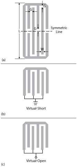
Figure 1 ILR layout (a) odd-mode equivalent circuit (b) even-mode equivalent circuit (c).
A balanced-to-unbalanced diplexer using interdigital line resonators (ILR) reduces circuit size and realizes high common mode rejection. By converting a symmetric four-port balanced bandpass filter (BPF) to a three-port device, a balun BPF with high selectivity and compact size is accomplished using ILRs. Then, a balanced-to-unbalanced diplexer is constructed by combining two balun filters with two 50 Ω matching lines. The balanced-to-unbalanced diplexer with operating frequencies at 1.8 GHz and 2.45 GHz exhibits excellent in-band performance, high selectivity and good isolation.
In modern communication systems, multifunction devices are desirable because they enable smaller and lower cost circuits. The balun diplexer is such a device, featuring both a diplexer filtering function and a balanced-to-unbalanced conversion function. Several three-port balun bandpass filters (BPF) that integrate BPFs and balun functions have been reported.1-3 Relatively little research has been done on balun diplexers, however. Bao et al.,4 and Wu et al.,5 report on unbalanced-to-balanced diplexer designs with one single-ended port and two balanced ports. These examples, however, are unbalanced-to-balanced diplexers that can only connect a single-ended antenna with differential receiver/transmitters. To function as an interface between a differential antenna and single-ended receiver/transmitter, a balanced-to-unbalanced diplexer is needed.
This article describes a new balanced-to-unbalanced diplexer with compact size, high isolation and good common-mode suppression through the use of ILRs. The design process includes three steps. First, the ILR is analyzed for its application in balanced BPFs. Second, a balun BPF with specific performance is realized by conversion from a four-port balanced BPF. Finally, two balun BPFs are combined with a 50 Ω tee to implement a balanced-to-unbalanced diplexer.
Property of an ILR
The ILR layout is shown in Figure 1a. Since it is symmetric along the dashed line, the odd-even mode approach is used to analyze its resonant behavior. The odd-mode and even-mode equivalent circuits are illustrated in Figures 1b and 1c. The odd-mode circuit is treated as a hybrid resonator, resonating at fdd.Compared to conventional quarter- and half-wave resonators, the ILR can operate at a lower resonant frequency, providing a size reduction benefit. On the other hand, the even-mode circuit can be considered a multi-open stub loaded resonator, resonating at fcc.
Because fcc is much higher than fdd,high CM suppression can be achieved. To verify this, an ILR is simulated on RT/Duroid 5880 substrate (h = 0.508 mm, εr =2.2 and tan σ=0.001),the same material used throughout the remainder of the development. The resonant frequencies simulated using Mentor Graphics’ IE3D are shown in Figure 2.
Balun Filter Design Utilizing ILRs
It has been shown that a three-port balun filter can be implemented from a symmetric four-port balanced filter with one of the ports being open.6,7 The four-pole balun BPF, composed of four compact ILRs, is shown in Figure 3 (W1=1.5, W2=0.5, L1=4, L2=4.1, L3=7.2, L4=6.75, L5=11.5, G1=0.2, G2=0.2, G3=0.8, H1=1.74 and H2=3.25. Unit: mm). Port 1 on the left side is the unbalanced port, and port 2 on the right side is the balanced port. The structure is symmetrical to the symmetry line, except for the unbalanced port. The balanced ports 1+,1-(diagonal filling portion) on the left side are used to show what a balanced filter should be and illustrates the relationship between a balanced filter and a balun filter. Since the balun filter is transformed from a balanced bandpass filter, the first step in the design of the balun filter is to design a balanced filter. For the DM response, a fourth-order Chebyshev filter is employed with a fractional bandwidth of 5 percent and a center frequency of 2.45 GHz. The ideal DM external quality factor and coupling coefficients are
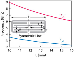
Figure 2 ILR simulated CM and DM resonant frequencies with different values of L, where W=0.5 mm and G=0.2 mm.
In the DM excitation, the symmetric plane is a virtual short. The center frequency of the DM passband is determined by Figure 2. The tap positions and gaps affect the Qe and coupling coefficients, respectively. The DM coupling coefficient and Qe are extracted,7 and their values with respect to structure parameters are shown in Figure 4. In the balanced filter design, simulation is accomplished with the IE3D full-wave simulator as well.
After obtaining the respective parameters using Equation 1, and Figure 4, the DM response is simulated and optimized. Under CM excitation, the symmetric plane is a virtual open. The resonant frequency is decided by Figure 2. The CM resonant frequency is much higher than the DM frequency; therefore, the CM response is strongly suppressed near the DM passband.
To transform the balanced filter into a balun filter, one side of the balun filter should be an unbalanced port, and the other side should be a pair of balanced ports. For the balun filter to have almost the same response as that of the balanced filter, the tap position of the balanced port should not be changed. However, for the unbalanced port, the tap position should be tuned to meet the external quality factor requirement
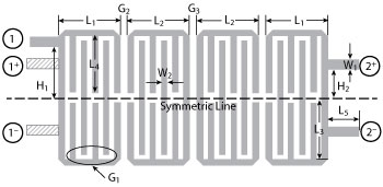
Figure 3 Balun filter structure using symmetric ILRs.
where  is the external quality factor at the unbalanced port.
In this balun filter design, the extracted with respect to the tap position is extracted in Figure 4 as well. With the tap position set to be 3.25 mm, a good balun filter response is obtained. Simulated and measured results are shown in Figure 5. Good agreement and high performance are observed.
Balanced-to-Unbalanced Diplexer
Based on the above approach, a second four-pole balun filter with 7 percent fractional bandwidth and a 1.8 GHz center frequency is designed. Then, the balanced to unbalanced diplexer is constructed. Figure 6 shows the configuration of the balanced-to-unbalanced diplexer, where the common Port 1 is balanced and Ports 2 and 3 are single-ended. To achieve high isolation and high return loss, the reflection coefficients  and
and  in Figure 6 should satisfy
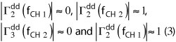
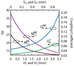
Figure 4 Extracted differential Qe and the Mij with respect to corresponding balun BPF physical parameters.
These requirements are easily realized by tuning the reflection group delay to make the common port group delay values equal to the individually synthesized values at the center frequency of both channels. After several optimizations, final dimensions are obtained (L1=4, L2=4.1, L3=9.66, L4=9.16, L5=12.5, L6=3.5, L7=2, L8=4, L9=4.1, L10=4.1, L11=4.0, L12=6.55, L13=7.55, G1=0.23, G2=0.97, G3=0.23, G4=0.31, G5=1.16, G6=0.37, G7=0.2, W1=1.5, W2=0.5, H1=3.76, H2=4.03, H3=1.8 and H4=3.01. Unit: mm).
Experimental Results
Good agreement between measured and simulated responses of the balanced-to-unbalanced diplexer is shown in Figure 7. The passbands are located at 1.8 GHz and 2.45 GHz with 3 dB bandwidths of 7.2 percent and 5.3 percent, respectively (see Figure 7a). The minimum insertion loss for each of the two channels, including SMA connectors, is 2.1 dB and 2.4 dB. Balanced performance is shown in Figure 7b. The maximum amplitude error is 0.5 dB and the maximum phase error is 2ºin the two operating bands. A photograph of the balanced-to-unbalanced diplexer is shown in Figure 7c. It is very compact at 34 mm ×9 mm (0.28λg ×0.40λg), where λg is the guided wavelength at 1.8 GHz.
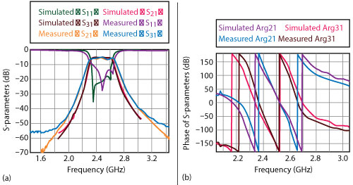
Figure 5 Balun BPF simulated and measured responses; amplitude (a) phase (b).
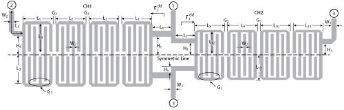
Figure 6 Balanced-to-unbalanced diplexer structure.
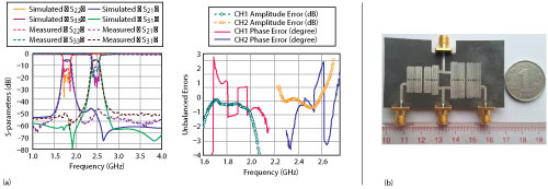
Figure 7 Diplexer simulated and measured responses (a) balanced performance (b) photograph (c).
Conclusion
A novel ILR is used to design a balanced-to-unbalanced diplexer. The resonator is compact and enables a large frequency separation of the DM and CM passbands. A balanced-to-unbalanced diplexer with operating frequencies at 1.8 GHz and 2.45 GHz is designed, fabricated and measured. Excellent in-band balanced performance, high selectivity and isolation are achieved.
Acknowledgments
This work was supported by the National Natural Science Foundation of China (NSFC) under project no. 61471292,no. 6133100,no. 61471388,no. 61001039 and the 55th China Postdoctoral Science Foundation Grant.
References
- Y.C. Leong, K.S. Ang and C.H. Lee, “A Derivation of a Class of 3-Port Baluns From Symmetrical 4-Port Networks,” IEEE MTT-S International Microwave Symposium Digest, Vol. 2, June 2002, pp. 1165–1168.
- D.W. Yoo, E.S. Kim and S.W. Kim, “A Balance Filter With DC Supply for BluetoothTM Module,” European Microwave Conference Proceedings, Vol. 2, October 2005, pp. 1239–1242.
- L.K. Yeung and K.L. Wu, “An LTCC Balanced to Unbalanced Extracted-Pole Bandpass Filter With Complex Load,” IEEE Transactions on Microwave Theory and Techniques, Vol. 54, No. 4, April 2006, pp. 1512–1518.
- Z.H. Bao, J.X. Chen, E.H. Lim and Q. Xue, “Compact Microstrip Diplexer With Differential Outputs,” Electronics Letters, Vol. 46, No. 11, May 2010, pp. 766–768.
- C.H. Wu, C.H. Wang and C.H. Chen, “A Novel Balanced to Unbalanced Diplexer Based on Four-Port Balanced-to-Balanced Bandpass Filter,” European Microwave Conference Proceedings, October 2008, pp. 28–31.
- Y.C. Leong, K.S. Ang and C.H. Lee, “A Derivation of a Class of 3-Port Baluns From Symmetrical 4-Port Networks,” IEEE MTT-S International Microwave Symposium Digest, June 2002, Vol. 2, pp. 1165–1168.
- J.S. Hong and M.J. Lancaster, “Microwave Filter for RF/Microwave Application,” Wiley, New York, 2001.
Jianzhong Chen received his B. Eng. degree in information engineering from Xi’an Jiaotong University, Xi’an, China in 2007 and his Ph.D. in microwave technology from Xidian University, Xi’an, China, in 2013.He is currently working with the Laboratory of Antennas and Microwave Technology at Xi’an Jiaotong University. His research interests include electromagnetic compatibility, design of antennas and microwave circuits.
Jie Shen received his B. Eng. degree in electrical engineering from Xi’an Jiaotong University, Xi’an, China in 2012 and is currently working towards his master’s degree in microwave technology at Xi’an Jiaotong University. His research interests include electromagnetic compatibility, optimization and microwave device design.
Ni Gao received her B. Eng. degree in electrical engineering from Xi’an Jiaotong University, Xi’an, China, in 2012, and is currently working towards her master’s degree in microwave technology at Xi’an Jiaotong University. Her research interests include microwave engineering design, modeling and optimization.
Anxue Zhang received his Ph.D. in electromagnetic field and microwave technology in 2003 from Xi’an Jiaotong University. From 2008 to 2009, he worked at Auburn University, in Auburn, Ala. as a visiting scientist. He has been a professor and Ph.D. student advisor at Xi’an Jiaotong University since 2013. His research interests include microwave engineering design, modeling and optimization.