
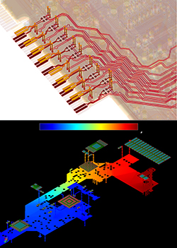
Design engineers face an incredible array of challenges to deliver multi-gigabit data rates for high performance consumer products, network infrastructure and devices that have become so commonplace. Savvy consumers expect that these devices and systems will work as promised. Making that possible, however, requires reliable high speed links. That means engineers have to perform a remarkable number of signal integrity (SI) and power integrity (PI) simulations and analyses, often as two separate design tasks. Keysight Technologies recently introduced two innovative technologies in the newest version of its Advanced Design System (ADS) electronic design automation software —ADS 2016 —that have redefined SI and PI analysis, by creating a cohesive workflow for both tasks that delivers higher accuracy and faster results (see Figure 1).
SI and PI are critical contributors to the quality and reliability of devices and systems. Engineers who don’t accurately simulate and analyze their designs may fail to identify and address problems early and risk their devices and systems not performing as expected in the field. Many hours troubleshooting an intermittent problem on the bench, trying to find the root cause, could easily have been identified by simulation. Crosstalk and stub resonances are usual suspects.
The challenge is that while SI and PI are closely interrelated design tasks with the same end goal — to ensure high speed link performance and system-level reliability — they are typically treated as separate design tasks. Usually they are performed using separate, general-purpose electromagnetic (EM) design tools, possibly from different simulation vendors. The key disadvantage of this approach, beyond the sheer cost of each point tool, is that the design engineer has to learn two different interfaces. During the design process, the engineer must switch back and forth between the tools, a time consuming and error-prone process. Because the two analyses may be performed by different engineers using different tools, collaboration is difficult at best. A further complication — engineers typically have to spend hours manually simplifying or reducing the size of their designs, since general-purpose EM tools have limited capacity and speed. Often, this is accomplished through a slow and cumbersome process of “cookie cutting” and removing layers and nets.
FASTER AND MORE ACCURATE
Unlike today’s general-purpose EM design tools, ADS’s new SIPro and PIPro solutions are specifically designed to help SI and PI engineers improve high speed link performance in printed circuit board (PCB) designs. SIPro focuses on enabling full EM analysis and model extraction for high speed links on large, complex PCBs. PIPro is used for full EM analysis of power distribution networks (PDN), including DC IR drop, AC PDN impedance and power plane resonance analysis. Both solutions are utilized within the ADS environment and deliver faster results than general purpose EM tools, while maintaining high accuracy.
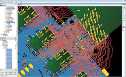
Figure 1 The newest version of ADS includes SIPro and PIPro, which provide a cohesive workflow in one environment.
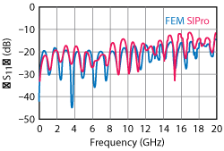
Figure 2 SIPro achieves accuracy approaching 3D EM solvers, yet in much less time. In this case, the 3D EM simulation took 12 min per frequency and consumed 8 GB of memory, while the SIPro analysis took 6 sec per frequency and required only 1 GB of memory.
SIPro utilizes a composite EM technology to ensure high frequency accuracy and the speed and capacity needed to analyze densely-routed, advanced PCB designs. Through simulation, engineers can characterize “all at once,” i.e., the loss and coupling of signal nets, power nets and complete ground nets. Via-to-via coupling and via transition effects can also be characterized, and ground return paths, cut-outs and drills in ground/power planes are accurately modeled. The accurate, extracted EM model seamlessly flows into an ADS transient simulation and channel simulation for complete channel analysis. Since SIPro is based on a net-driven use model geared for SI and PI, it is much faster to set up and much more efficient than general-purpose EM tools. Because it leverages multiple EM technologies, it delivers accuracy approaching that of industry-standard 3D EM solvers — something that can be achieved in just a fraction of the time it would take to complete a full-wave 3D EM simulation. When compared to finite element method (FEM) simulation, the industry’s gold standard, it demonstrates very good agreement at a small fraction of the time and memory consumption, even at high frequencies (see Figure 2).
Like SIPro, PIPro is an EM-based solution. It provides accurate and efficient net-driven analysis utilizing three specialized simulation engines. A DC IR drop simulator provides a table of DC voltages and currents for each via, pin, sink and voltage regulator module in the PDN. Using this information, engineers can predict the DC voltage at the pins of the ICs sinking the current. A 3D visualization of the design’s voltages, current density and power dissipation on the power and ground nets enables engineers to easily identify trouble spots in the PCB (see Figure 3). With the AC PDN impedance simulator, the frequency dependency of the PDN can be calculated with decoupling capacitors (decaps) in place. After tuning decap values, the PDN impedance can be quickly re-analyzed without additional EM simulations. The resulting S-parameter model extraction of the PDN can be back-annotated to the schematic, along with circuit models of the components, to enable further tuning and optimization. Additionally, the simulator provides greater visibility into the PDN with its 3D field and current density plots. A power plane resonance simulator can be used to identify the PCB layout’s self-resonant frequencies. It also helps engineers visualize the PCB’s electric and magnetic fields to better understand where resonances are originating. Layout areas with the highest field strength can be further examined, aiding the placement of decaps.
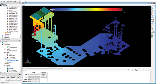
Figure 3 PIPro provides 3D visualization of voltages, current density and power dissipation on the power and ground nets.
COHESIVE WORKFLOW
A key benefit of ADS’s new SIPro and PIPro solutions is that they share the same analysis environment,including a common GUI, workflow, model database and visualization results via a native 3D viewer. This allows engineers to visually inspect nets prior to simulation and view post-processed field visualizations in 3D; it also creates a cohesive workflow for both SI and PI design tasks (see Figure 4). Rather than having to switch between point tools, engineers can now use asingle user interface for both PI and SI analyses. One EM setup can be easily copied from one analysis to the other and vice versa, with simulations run in the same environment.
The setup itself is completely net driven. This allows engineers to select only those nets they want to simulate, with no engineering effort or time required to manually manipulate layout objects prior to simulation. With the high capacity EM solvers in SIPro and PIPro, engineers can tackle more nets at once. With ADS’s cohesive new workflow, engineers can literally go from layout to results in less than 20 clicks. The workflow automatically generates schematics to prepare EM models for immediate use with ADS’s channel, DDR bus and transient simulators. Using them, engineers can perform SI analyses (e.g., BER contour measurements) and complete design verification with standard-specific compliance test benches.
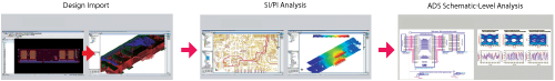
Figure 4 ADS’s new cohesive workflow redefines SI and PI analyses by eliminating the limitations from treating SI and PI as separate design tasks and using general-purpose EM tools for analysis.
Conclusion
Accurate signal and power integrity analyses are critical to ensuring optimal high speed link performance in PCBs. While general-purpose EM tools can be used to accomplish these tasks, the process requires much more manual intervention and is not conducive to engineering collaboration. ADS’s new SIPro and PIPro solutions overcome these limitations with powerful new EM technology that delivers accuracy approaching industry-standard 3D EM solvers, while delivering results in a fraction of the time. A cohesive workflow seamlessly transfers EM characterized models back into the schematic and promotes better collaboration. Together, these capabilities raise the bar on performance, accuracy and efficiency for SI and PI simulation and analysis. Design engineers now have the capabilities they need to address their toughest design challenges in the fastest way possible.
Keysight Technologies Inc.
Santa Rosa, Calif.
www.keysight.com