

Editor’s Note: As time-to-market demands have increased and modeling/measurement systems have become more complex and difficult to assemble, companies have been seeking fully integrated, turnkey system solutions. Microwave Journal asked some leading software and measurement companies to review their offerings in this area including their advantages for customers. Keysight Technologies, National Instruments, Maury Microwave and Focus Microwaves review their capabilities in the area of integrated modeling/measurement solutions, many made up of software and hardware components from multiple companies teaming up to offer a full turnkey system solution.
Turnkey Solutions for Semiconductor On-Wafer Measurements
Yoshiyuki Yanagimoto,
Keysight Technologies, Santa Rosa, Calif.
As semiconductor technology continues to evolve, time-to-market cycles are shrinking and the need for even greater accuracy is increasing. Unfortunately, those trends often run counter to the need to properly characterize semiconductor components and devices during their development and manufacture. One issue is the time that is required to configure and assemble a measurement system to handle this task. In a typical wafer-level measurement system for mmWave measurements, for example, over 25 to 30 cables must be properly configured and assembled. The semiconductor test engineer may spend several months evaluating, ordering, assembling and verifying that system. And because it is so complex, there is a greater likelihood that a cable,connector or mechanical component will be missed, further delaying its commissioning.
The software used in the measurement system can also create challenges for the engineer. Such systems, which typically include a probe station, measurement instruments and calibration, are generally controlled by multiple pieces of software. That means that the engineer is forced to deal with different user interfaces just to operate one system. Even highly skilled engineers have to spend months or even years working to establish measurement automation. According to one recent customer survey, the need for a software solution capable of efficiently controlling both the prober and instruments, while maintaining the necessary flexibility to address diverse measurement needs, was identified as a “top three” priority.
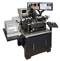
Figure 1 Typical WMS configuration with Keysight measurement instruments and Cascade Microtech probe station.
These challenges demand an integrated, turnkey system that can quickly and accurately perform advanced DC, RF/microwave/mmWave, high power and flicker noise measurements on semiconductor components and devices. Keysight Technologies and Cascade Microtech set out to deliver this type of system in June 2014 and launched wafer-level measurement solutions (WMS). WMS provides fully configured and validated RF measurement solutions to satisfy the ever increasing demands, both technically and volume-wise, of on-wafer measurements (see Figure 1). To date, over 80 configurations have been tested and over 1,800 calibrations performed. Since WMS was first announced, an increasing number of semiconductor test engineers developing and manufacturing semiconductor components and devices are asking for a complete solution, rather than a collection of individual parts from various suppliers.
Integrated, TurnKey Solution
Providing an answer to that demand for a “solution,” the WMS program delivers a turnkey solution for on-wafer measurements through three key deliverables: guaranteed configuration, guaranteed installation/verification and guaranteed support. These deliverables are critical to ensuring the measurement system is not only turnkey, but can quickly and accurately make the measurements today’s semiconductor test engineers demand.
With guaranteed configuration, Keysight and Cascade Microtech also guarantee that if there is a missing piece in the delivered system, it will be provided free of charge. One way they ensure a complete system is delivered is through a three-way joint meeting; essentially a Keysight/Cascade Microtech sales team meeting that takes place with the engineer at the beginning of any new engagement. The three-way joint meeting eliminates the need for the engineer to meet with the sales teams from each company separately. This is not only a much more efficient use of time, but makes sure that the end system will satisfy the engineer’s needs with the most reasonable and reliable configuration. It also helps ensure that there are no missing components in the system or careless mistakes made; something which can easily occur when different parties are involved in separate meetings.
Guaranteed installation allows engineers to request a variety of services at purchase, such as installation service, on-site functional qualification, measurement consultation, application training, and complete system verification and performance —all provided by application experts. These services eliminate the headaches and worries an engineer normally faces when installing a measurement system and drastically shortens the time-to-first measurement. Keysight’s WaferPro Express software was specifically designed to enable engineers to quickly setup and execute automated measurements, as well as the system performance verification. The WMS program’s guaranteed support means that engineers gain a single point of contact for support, rather than having to wonder which company to contact when a system level issue is encountered.
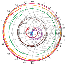
Figure 2 The Keysight Verification Substrate verifies a system with a higher coverage of the Smith Chart.
Pre-Configured System Option
To further simplify the process of making on-wafer measurements and speed the actual time-to-first measurement, the companies spent a tremendous amount of time evaluating commonly used combinations of measurement instruments, including Keysight’s B1500A Semiconductor Device Parameter Analyzer, N6705B DC Power Analyzer, PNA and PNA-X Network Analyzers and mmWave Extenders, and Cascade Microtech’s multiple probe stations (e.g., the SummitTM/Elite300TM/CM300 series probe stations) and probes (e.g., Infinity® probes). As a result of these efforts, a number of pre-configured systems are now available with guaranteed performance. When one of these systems is purchased, the companies provide a system specification that serves as an acceptance criteria at installation.
Enabling System Performance Verification
A key benefit of the WMS program is that the complete on-wafer measurement system performance is not only specified, but verified during installation. As an example, the WMS program verifies the DC leakage and noise of the entire system. Previously, DC leakage and noise could only be specified separately at the front connectors of the Keysight B1500A Semiconductor Device Parameter Analyzer by itself and at a stand-alone Cascade Microtech probe station.
For RF measurements, an application expert performs S-parameter verification at the tips of the probes using a newly developed Keysight verification substrate (KVS) up to 110 GHz.
The KVS contains multiple devices, such as a mismatch line (Beatty Standard) and 25 and 100 ohm series resistors, as well as the open, short, load and line standard to more confidently verify S-parameter measurements (see Figure 2).
One reason KVS is able to produce a more confident verification is that its verification standards cover a wider area of the Smith Chart. In contrast, traditional verification uses the open, short, load and line standard, which only runs on the outer circle of the Smith Chart or stays at the center dot, making it much more limited. By verifying the complete measurement system using KVS and via DC leakage and noise, engineers gain greater confidence in the overall performance of their measurement system.
Reducing Measurement Setup Complexity
Keysight and Cascade Microtech jointly developed a software platform that interfaces with all the needed pieces of an on-wafer measurement system. Called WaferPro Express, the platform enables automated characterization of wafer-level devices and circuit components (see Figure 3). It features over 50 measurement turnkey drivers and many test examples so that an engineer can immediately perform the needed measurements. Engineers can start an operation and write an automation program without having to waste time learning multiple pieces of software. By efficiently controlling all of the components in a wafer-level measurement system—instruments and wafer probers—WaferPro Express is able to reduce the engineer’s measurement setup complexity and provide a unified platform for efficient automated measurement and data management.
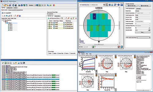
Figure 3 WaferPro Express software enables turnkey automated measurements as well as full customization.
With its guaranteed configuration, installation/verification and support, KVS-enabled verification and WaferPro Express software, the WMS program offers a compelling turnkey solution for on-wafer measurement needs; whether being performed on the semiconductor factory floor or by R&D teams measuring high-volume data for applications such as device modeling, process monitoring, reliability and component characterization. Engineers performing such tasks can no longer afford the time it would normally take to evaluate, order, assemble and verify a traditional measurement system. For today’s semiconductor test engineers, the benefits of the WMS program are accurate and repeatable testing, faster time-to-first measurement, and assured data correlation between multiple locations—all of which are essential to allowing today’s semiconductor test engineers to perform accurate and fast advanced DC and RF measurements on both components and devices to get their products to market on time.
Customized Advanced Modeling through PXI-Based High Speed Nonlinear Measurement Systems
David Vye and Marc Vanden Bossche, National Instruments, Austin, Texas
Device modeling, specifically transistor characterization at RF frequencies and above, has been the ongoing focus of R&D for well over 40 years. Initially driven by early mil/aero funding for MMIC development, device modeling enables design innovation by bridging the gap between known transistor technology (through measurement) and unknown circuit performance (through simulation). In the earlier days of device characterization and circuit design, measurement technology, equation-based predictive modeling and simulation took shape through a mix of independent and collaborative efforts to characterize and predict the electrical behavior of new semiconductor processes.
Today, the goal for the device modeling remains the same: support basic device development and provide the design engineer with an accurate representation of how that device will behave when operating within the design network under real-world conditions. As RF semiconductor technologies mature, many transistor development and modeling techniques will be addressed with existing commercial turnkey solutions. For newer semiconductor technologies targeting applications that require models based on a broader characterization region (i.e., wideband, dynamic, thermal), the need to advance measurement speed, accuracy and customization will continue.
Device Modeling
Understanding the factors driving development in device characterization starts with an examination of how data is measured and used to create predictive models. The three most common types of models used are physical models, compact models and behavioral models. Models for silicon devices such as BJTs and CMOS are commonly based on semiconductor physics. Industry standard compact models for compound semiconductor such as GaAs and GaN are typically based on empirical equations describing currents and charges as a function of the applied voltages and temperature. Behavioral models use direct measurements to represent the device with component responses to specific controlled stimuli captured in a “black-box” table or data file.Behavioral models are only valid under the operating conditions measured. This model type is actively under development and has recently been improved to take memory effects into account.
The compact transistor model is widely used to model the III-V semiconductor devices which are the mainstay of RF/microwave applications. Compact models extracted from measured IV, quasi-isothermal pulsed IV, S-parameters and pulsed S-parameter data, with validation from load-pull characterization, can take into account complex phenomena such as electro-thermal and trapping effects. Most of today’s PAs are fed by modulated signals such as versatile pulses in the case of radars or highly modulated signals in the case of telecommunication applications. It is essential to assess the dynamic behavior of RF devices fed by these large modulated signals. Contrary to CW conditions, low frequency and high frequency memory effects created by trapping and thermal effects must be included to accurately predict the device response to complex modulated signals (such as EVM or ACPR).
To accurately predict RF (and digitally modulated) nonlinear behavior, advanced compact and behavioral models require a considerable amount of measured data, which significantly increases the time it takes to fully characterize a single device and validate the model through load-pull verification. Rapid measurement systems are required to reduce data acquisition time and to make the modeling practical. Today, the speed and flexibility of PXI-based systems make it practical to obtain massive data sets for device modeling, targeting design work as well as production test.
Modular Platform Solution
PXI is a PC-based platform for measurement and automation systems that are compact, fast, cost-effective, adaptable and accurate, and enable many features that were previously available only to high-end and expensive setups. National Instruments supports the development of state-of-the-art device characterization systems through cooperation around solutions from Maury Microwave, Anteverta-mw (now part of Maury Microwave), Focus Microwaves and Mesuro (now part of Focus Microwaves). For these load-pull solutions, vendors are combining their expertise with NI PXI hardware and system design software, like LabVIEW, to overcome the increasingly time-consuming source and load-pull characterization requirements placed on microwave power amplifiers.
Load-pull characterization is an essential tool to increase the efficiency of power amplifiers. Due to time and cost, vendors have historically performed load-pull only during design. Today, however, the speed and flexibility of a PXI-based system make it possible to verify power amplifier performance during design verification and production test (see Figure 4).
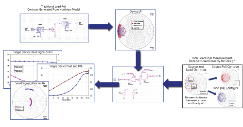
Figure 4 New design flow replacing load-pull contours generated from nonlinear models with direct load-pull measurement sets.
The LabVIEW reconfigurable I/O (RIO) architecture is part of the NI PXI platform. It includes the latest computing technologies, such as multicore CPUs and FPGAs, and a single, common development approach and language. Maury, Focus and their acquired companies are benefitting from this architecture, along with their unique approaches, to help their customers simplify test and decrease time to market.
Maury Microwave (with Anteverta), utilizes the high speed and broadband modulation capabilities from the NI PXI form factor to create a solution that is ideal for power amplifier characterization during development, pre-production and production testing. These systems allow broadband impedance synthesis which is becoming more important to design power efficient and linear amplifiers. The resulting large amount of test data can be managed through NI’s LabVIEW, which is a graphics-driven programming environment for developing test systems. It is possible to compress all the data into a measurement-based behavioral model which can then be used with NI AWR Design Environment for circuit design.
Using the latest generation of commercial, off-the-shelf NI PXI hardware, Focus (with Mesuro) developed its RAPID load-pull system that employs a “quasi closed loop” approach, which maintains the speed of a closed loop active load-pull system but removes the inherent stability issues that limit its application. The output signal from the device is fed to a circulator or coupler and passed to the PXI chassis, where the signal is down-converted, modified to set the desired impedance, up-converted and then injected back to the test device to set an invariant impedance. Due to the system feedback, changes in the device output due to a drive level shift will be automatically compensated for in the feedback signal. This results in extremely fast impedance changes and a fast calibration process.
Even the use of a passive tuner in combination with the PXI-based vector signal transceiver (a combination of a VSG, VSA with a common FPGA architecture) and possibly a PXI SMU, speed up the classic source and load-pull. LPLite is an open-source
LabVIEW application, provided by NI as reference architecture that supports an intuitive source- and load-pull application using passive tuners from both load-pull companies. LPLite stores this characterization data away in a NI/AWR compatible data format. This reference architecture can be extended easily with ET and DPD where again one benefits from the synchronization and speed of the PXI. All of these options provide a flexible system that can meet the needs of most any engineer.
Addressing Time-to-Market with Turnkey Measurement
and Modeling Systems
Steve Dudkiewicz, Maury Microwave, Ontario, Calif.
As companies become more vertically integrated, they take on greater responsibilities for accurate and robust device modeling and associated measurements across multiple product levels (IC, die, package, etc.). With time-to-market an important organizational goal, the need for a highly efficient, turnkey component-to circuit-to system-level measurement and modeling device characterization solution has never been more critical. Maury Microwave and AMCAD Engineering have partnered to address this need with a turnkey design flow (see Figure 5) that includes the instrumentation and software necessary to take measurements and extract, validate and refine compact and behavioral models, all from within a single intuitive software platform.
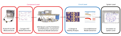
Figure 5 Design flow to extract component- and circuit-level compact and behavioral models.
Transistor Models
The first step in developing a comprehensive line of state-of-the-art transistors is to create highly accurate and reliable compact transistor models. Compact models include elements associated with linear, nonlinear, electro-thermal and trapping circuits and are extracted from synchronized pulsed IV/S-parameter measurements using an AMCAD BILT pulsed IV system, Keysight PNA-X and Maury IVCAD software suite (see Figure 6). Linear compact models are extracted using S-parameters to determine the extrinsic parasitic elements, from which the resulting data is used to extract frequency-independent intrinsic parameters.
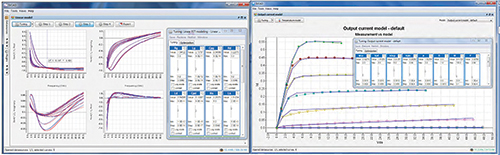
Figure 6 Linear and nonlinear model extraction optimization in IVCAD.
Nonlinear model extraction uses pulsed IV measurements to study the effects of temperature-dependent performance in safe operating regions and to study the breakdown area of a transistor. Pulse widths and duty cycles are chosen to maintain quasi-isothermal operating conditions. Pulsed IV measurements are used to extract the current diodes, and synchronized pulsed IV/S-parameters to extract the nonlinear capacitance model.
Electro-thermal circuits are used to model transistor performance as a function of device temperature and device self-heating. A transistor’s thermal resistance is extracted using the differentiation between continuous and short-pulsed bias conditions. Thermal capacitance is extracted using longer pulses and studying current decrease with time. Thermal impedance is modeled from several thermal resistances and capacitances representing various time constants.
Trapping effects, surface trapping (gate lag) and buffer-trapping (drain lag) are modeled from sets of pulsed IV measurements at multiple quiescent bias points. Quiescent bias points are specifically chosen such that the difference between IV characteristics can be entirely attributed to either gate or drain lag.
Model Validation
Following the turnkey compact model extraction flow, the 58 electrical equivalent parameters are automatically determined and result in ready-to-use III-V or MOS compact transistor models. Since the nonlinear compact transistor model was extracted from linear S-parameter measurements, nonlinear vector-receiver load-pull (see Figure 7) can be used to validate and refine the model based on nonlinear fundamental and harmonic load-dependent measurements as a function of impedance, power compression and bias.
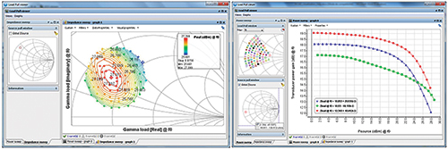
Figure 7 Load-pull iso-contours and gain compression curves under nonlinear operating conditions.
Vector-receiver load-pull uses a VNA to measure frequency-selective a- and b-waves from which separate and accurate fundamental and harmonic input and output powers are calculated. Since the large-signal input impedance of the transistor is measured in real-time, delivered input power can be calculated as well as operatingpower gain and gain compression that are directly related to the intrinsic transistor’s performance independent of source match. Vector parameters such as AM/PM and droop, and multi-tone parameters such as intermodulation distortion products and intercept points can be measured and compared against simulated data.
Certain VNAs, such as Keysight PNA-Xs, allow for nonlinear VNA time-domain voltage and current waveforms to be measured. When de-embedded to the intrinsic transistor reference plane, measurements can be compared against simulated data and used to refine and enhance the compact model.
CW and pulsed-RF powers can be swept using programmable signal sources to study the device’s performance under small-signal to highly-compressed operating conditions. DC and pulsed biases can be adjusted using programmable power supplies or pulsed-bias (pulsed IV) systems. Impedances can be presented at the fundamental and/or harmonic frequencies using Maury’s LXITM certified passive single or multi-harmonic automated impedance tuners, active tuning chains or a combination of both. Nonlinear vector-receiver load-pull plays a critical role in validating any nonlinear model by presenting actual nonlinear operating conditions to the modeled transistor, and is useful for refining the model as needed.
Behavioral Models
Once a nonlinear compact model has been extracted, or if a compact model is unavailable, it is often useful to have a component-level behavioral model available for circuit design use. Unlike compact models which expose the workings of the transistor, behavioral models are “black-box” and based on a behavioral response to a set of stimuli. Nonlinear load-pull measurement data can be converted to various behavioral models, including Keysight’s X-Parameters and AMCAD’s Enhanced PHD (EPHD). These models can be used to quickly simulate the behavioral response of a transistor and are useful for circuit design and evaluating the transistor performance versus operating conditions. Certain behavioral models, such as the AMCAD multi-harmonic Vollterra (MHV) model can be useful for system design, taking into account low frequency and high frequency memory effects and accurately simulate ACPR and EVM using wideband modulated signals.
Amplifier and MMIC designers will often find that their designs suffer from spurious oscillations, only discovered after a circuit has been fabricated — resulting in the necessity of multiple spins. To avoid costly redesigns, stability analysis is an important step in the design flow, and STAN (STability ANalysis) can determine the nature of oscillations under both small-signal and large-signal operating conditions. Based on the pole-zero identification technique, oscillations are analyzed as a function of bias, power, impedance and manufacturing tolerances at multiple nodes of a circuit. Without a single fabrication, oscillation avoidance using the minimum number of stabilization networks can be compared against RF performance and result in the ideal compromise, leading to first-pass design success.
Without a single software platform covering the entire design flow, one runs the risk of incompatible formatting, missing measurement data and lost time. IVCAD (see Figure 8) is a single suite which includes modules for synchronized pulsed IV and pulsed S-parameter measurements, compact transistor model extraction for III-V and MOS technologies, passive, active and hybrid-active fundamental and harmonic load-pull for model validation, refinement and design, multiple behavioral model extraction techniques, stability analysis of microwave circuits, with advanced visualization and data analysis, full scripting and automation capabilities. IVCAD measurement, compact model and behavioral model file formats are compatible with commercial simulation tools for easy transition from measurement and model to simulation.
Figure 8 IVCAD measurement and modeling device characterization software suite.
All-in-One Measurement and Modeling Systems
Vince Mallette, Focus Microwaves, Montreal, Canada
Today’s design engineers are looking for systems that can do it all. Integrated nonlinear measurement solutions can help designers generate compact models resulting from accurate linear pulsed S-parameters. They can also perform all the required measurements to generate a robust measurement-based behavior model calculated from wave-based harmonic load-pull measurements.
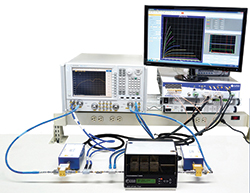
Figure 9 Auriga’s AU4850 high power Pulsed IV and MPT-5080 8 to 50 GHz multi-harmonic tuner driven by Focus’ and Mesuro’s device characterization software.
Load-pull measurements will continue to be an integral part in the design flow for RF and microwave power devices for the foreseeable future. Collection of a rich load-pull data set can shorten design cycles. Early last year, Focus added to their portfolio high power pulsed IV testing from AURIGA Microwave and behavior modeling tools from MESURO.
Pulsed IV
Depending on what model extraction method designers prefer, there are various solutions to reach the end result. Pulsed IV (current-voltage) measurements have emerged as one of the popular methods of capturing current-voltage characteristics of active devices such as field effect (FET) and bipolar junction (BJT) transistors. With the growing popularity of high-power devices, like GaN HEMTs, LDMOS, SiC and graphene, current and voltage requirements are being increased.
The Auriga AU4850 is a full-featured characterization platform capable of measuring DC IV and pulsed IV curves, expandable to pulsed S-parameters and pulsed load-pull. With rise times as fast as 30 ns, measurements can be made near the instant of activation to mitigate channel, self-heating and memory effects. With pulse widths as narrow as 70 ns, the system is well suited for isothermal testing of devices. Advanced in-situ calibration features allow for correction and accuracy at the DUT reference plane.
Load-Pull
Using the vector receiver architecture, fundamental and/or harmonic load-pull can be undertaken using a variety of configurations, either employing internal VNA sources or external RF sources and a PLL interface. Focus’ MPT series of wideband harmonic tuners simplifies and reduces the cost of highly complicated harmonic load-pull setups. Multi-purpose tuners (MPT) use three independent wideband probes, allowing independent control of the amplitude and phase of the reflection factor at all three harmonic frequencies. The MPT can be used to pre-match impedances at the fundamental and the harmonic frequencies to reduce amplifier power by an average factor of 10 dB, and the corresponding cost when used in active systems to reach the edge of the Smith Chart. The MPT can also be used for static passive harmonic tuning in a high speed active setup with a single fundamental injection source. The active harmonic load-pull setups configured this way are marketed as model HAILP (Hybrid Active Injection Load-Pull, with one injection source) and HAILP+ (with two or three harmonic injection sources). Figure 9 shows Auriga’s high power pulsed IV and 8 to 50 GHz multi-harmonic tuner, driven by both Focus’ and Mesuro’s device characterization software, performing the measurements and generating a device model — providing a complete measurement and modeling system.
behavioral models
Nonlinear measurement data has been exploited in various ways to create behavioral models for high frequency components. These include frequency domain descriptive behavioral models, such as poly harmonic distortion (PHD) models, S-function and Keysight’s X-parameters. Formulations of these models have been defined in terms of the travelling waves, with a desire to represent nonlinear behavior of high frequency transistors through a direct extension from the linear S-parameters. Figure 10 shows the results generated from an imported model.
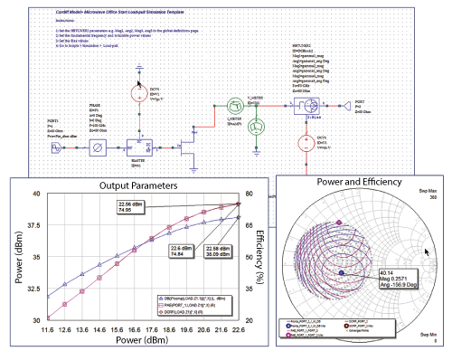
Figure 10 Example results generated from an imported model.
The Mesuro model portfolio has a number of solutions that range from the direct data look-up approach of the Cardiff DWLU model, for recreation of measured data; to the Cardiff Model Lite, where the desired output is a local model; to the Cardiff
Model+ formulation, which incorporates higher-order mixing terms with perfect accuracy over the entire impedance plan.
The Cardiff Model+ is a generalized solution using an nth order “mixing” parameter formulation that can be applied as a fundamental only mode or using the harmonic content and then easily extracted using the model generation tool and used within the EDA simulation environment. The measurement data can then be exported in a file format as required by the user, such as .XNP or .MDF, to be used within the available EDA tools.
The Cardiff Model+ is a poly-harmonic distortion (PHD) model. The ideal analyzing set is generated by varying one parameter at a time and analyzing the effect on the frequency components. The MPT tuner simplifies the control of three independent impedances at the given frequencies.
More than ever, a combination of companies like Focus Microwaves together with MESURO and
AURIGA are providing one-stop shopping for design engineers. If we go back only a few years the typical load-pull system was a scalar solution and was considered “high-end” when you could tune harmonics for a very narrowband frequency range. Now most systems delivered by Focus are compatible with the widest range of available instrumentation, offer a wide bandwidth, tune harmonics passively and actively both on the input and the output, support wave-based receiver measurements and are capable of producing robust behavior models.