
A Sub 1 W Load-pull Quarter-wave Prematching Network Based on a Two-tier TRL Calibration
Transistors used for cellular and PCS infrastructure applications are required to amplify signals with a peak-to-average ratio that can exceed 13 dB, resulting in a peak envelope power (PEP) approaching 1 kW. This PEP requirement is a consequence of simultaneous amplification of multiple digitally modulated carriers with a time-varying envelope and requires a load resistance in the neighborhood of 0.3 W. Present load-pull technology based on mechanical tuners is limited to approximately 1 W at cellular and PCS frequencies, which renders these systems incapable of characterizing transistors under these conditions. Quarter-wave prematching networks have been developed to transform the source- and load-pull domains to a lower impedance. A variety of techniques have been used to characterize these quarter-wave networks, including standard vector network analyzer (VNA) error correction. This article presents a further refinement of this characterization technique, which is based on a two-tier calibration using 7 mm and microstrip thru-reflect-line (TRL) calibrations.
John F. Sevic
Spectrian Corp.
Sunnyvale, CA
RF power amplifiers deployed with first-generation cellular base stations were based on cavity combiners and class C- operated silicon bipolar junction transistors for final-stage devices. Up to 10 independent carriers, each constituting one user, typically were combined prior to feeding the antenna. This architecture, coupled with the constant envelope property of FM, virtually eliminated the need for linear transistor operation. However, the linearity requirements placed on transistor performance for second- and third-generation wireless base stations are much more demanding. Wireless service providers require that base stations occupy as little volume as possible and, with the adoption of digital modulation, many carrier signals now have a time-varying envelope. The first requirement implies the elimination of the cavity combiner, thereby requiring simultaneous amplification of several carriers. The second requirement implies that quasilinear class AB amplification be used to maintain the integrity of the modulation envelope.
These changes have drastically changed the way in which high power transistors are characterized. Simultaneous amplification of several carriers, each with a time-varying envelope, results in a peak-to-average ratio that can exceed 13 dB, leading to a PEP demand approaching 1 kW. At the standard 26 V base station supply voltage, a load resistance in the neighborhood of 0.1 W is required for generating closed load-pull contours of power, gain, power-added efficiency and adjacent-channel power rejection.
Present high power load-pull technology is based on either active fundamental re-injection or mechanical tuners.1-4 Although in principle an active load-pull system can present an arbitrary load impedance, the architecture of these systems is not amenable to generating the extremely high power necessary to emulate a sub 1 W load at 1 kW PEP. The current state of the art in mechanical tuners is limited in resistance to approximately 1 W, although narrowband systems can go lower.5 To overcome the limitation posed by mechanical tuners, many researchers have adopted quarter-wave prematching networks to transform the tuner impedance to a lower impedance. With this approach, it is possible to present a sub 1 W resistance necessary for high power transistor characterization.
To enhance the accuracy and repeatability of load-pull characterization, it is essential that the pre-matching network be accurately characterized for de-embedding. Several methods are available to accomplish this task, including analytical methods based on approximate closed-form expressions, full-wave analysis using numerical techniques and employment of VNA error-correction theory.6-8 The first and second methods are based on approximations that have built-in uncertainty in the form of material parameter uncertainty. The third method is entirely measurement based and relies on well-behaved error-correction mathematics to remove the effects of the pre-matching network. More importantly, using verification standards, it is possible to quantify the accuracy and uncertainty of the de-embedding.
This article presents a two-tier calibration method based on 7 mm and microstrip TRL calibrations for characterization of a custom quarter-wave prematching network. This system is capable of presenting 0.1 W at 1900 MHz using model MT918B tuners.1 Verification results are given that demonstrate that source- and load-match error terms are better than -45 and -52 dB, respectively, from 0.85 to 3 GHz.
De-embedding and Characterizing Systematic Errors
Precise vector network analysis relies on the identification and de-embedding of systematic errors. Depending on the properties of the two-port device to be measured, certain error terms are more significant than others. For this analysis (a high reflectivity environment), the forward and reverse source- and load-match terms are the most significant. Here, the source and load match essentially are the corrected terminating port impedances of the DUT and, thus, directly impact the accuracy of impedance data extracted from measured S parameters. Figure 1 shows a signal-flow diagram of the forward path of a typical VNA with each of the standard error terms labeled. Note that although 12-term error correction can be used in three-sampler architectures, a four-sampler architecture is required here since TRL calibration is adopted.
 Figure 2 shows a graphical interpretation of source match. Zref is the reference impedance of the calibration; the uncertainty in Zref is denoted by the red circle at the center of the Smith chart. Consider now an offset short, which is represented as a vector of approximately unity length and a linear phase response with respect to frequency. Uncertainty in Zref is represented by the green circle near the left side of the Smith chart and is quantified by Esf, the forward source match (and Esr, the reverse source match). Due to the nature of the bilinear transformation, errors in source match are greatly magnified near high reflectivity regions of the Smith chart and directly result in significant measurement inaccuracy. Thus, the green circle represents a proportionally larger impedance uncertainty than does the red circle although each circle has the same radius. It is for this reason that forward and reverse source match are critical for high reflectivity measurements. A similar argument can be made for the forward and reverse load match.
Several calibration techniques have been developed to characterize and de-embed systematic errors encountered in contemporary vector network analysis. Of these, the TRL technique offers the best accuracy for source and load match.9-11 Since the TRL technique requires insertable calibration standards, the present fixture was designed in two dividable halves. Microstrip standards used for the fixture calibration constitute the first (inner) tier of the calibration. The second (outer) tier of the calibration is based on a 7 mm coaxial TRL calibration. Using adapter removal with MultiCal, these two calibrations characterize each fixture half.12 Figure 3 shows the reference plane definitions for each tier. The delay standards are denoted as Z1 and Z2 to indicate the reference impedance of each associated tier.
Transistor packages designed for use in high power applications generally have lead widths to match the impedance of the microstrip printed on the PCB, which is usually in the neighborhood of 10 W. Spectrian's 30 and 60 W laterally diffused metal-oxide semiconductor packages use a lead width of 215 mils; this dimension was chosen for the width of the microstrip used in the fixture and for the delay and verification standards. Note that since TRL calibration assigns the system reference impedance to be equal to the impedance of the delay standard(s), the S parameters of tier 1 must be renormalized to 50 W to maintain compatibility with the 50 W reference impedance used in standard load-pull software.1,2 This transformation is also performed with MultiCal, which requires that the impedance of the delay line be known.12 The propagation method of Marks and Williams was adopted to extract the characteristic impedance of the delay line of tier 1, which was determined to be 11.5 W from 0.1 to 4 GHz.13
With respect to the de-embedding methods discussed previously, the primary advantage of the method described here is the availability of verification standards to determine the corrected source- and load-match performance. Use of verification standards enables a measurement to be made of how close the corrected forward and reverse source and load reference impedances are to a known standard. Although this technique includes finite directivity leakage, it can be assumed that the reflected power is much greater than the coupled power due to finite directivity and, hence, can be ignored. In addition, the effect of frequency tracking is included, which will manifest itself as a generally negative slope in the verification response.
 Figure 4 shows the forward and reverse source match of the 7 mm TRL calibration. The forward and reverse source match, measured using a 50 W, 30 cm beadless airline terminated in a 7 mm short, are better than -53 dB from 0.85 to 3
 GHz. Figure 5 shows forward and reverse load match using the same delay line where it is determined that a better than -56 dB match is achieved (except near 0.85 GHz). This performance is typical of a model HP8510C/HP8514B microwave network analyzer using a 7 mm coaxial TRL calibration.8,9
Figure 6 shows the forward and reverse source match of the microstrip TRL calibration using a 6 cm, 11.5 W offset-short standard. The forward and reverse  source match are better than -45 dB from 0.85 to 3 GHz. Figure 7 shows the forward and reverse load match using a 6 cm, 11.5 W delay line. A better than -52 dB match is achieved over 0.85 to 3 GHz. (Information on extraction of error terms
 from verification data is provided by Balo.14 ) It is possible to frequency shift the calibration bandwidth by using a different delay line in tier 1 or to expand the frequency bandwidth using a multiline calibration.11
The good source- and load-match performance of the microstrip calibration provides a high degree of confidence in the fixture characterization. An alternative verification procedure, which also includes the effect of tuner repeatability (and the accuracy of the calibration used for the tuner 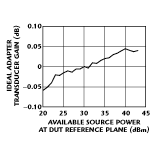 characterization), is to insert a thru in the load-pull system and perform a load pull around a known impedance. The simplest approach is to set one tuner to Z and the other to Z* and perform a power sweep. Based on swept power results with no fixture (representing direct connection of the tuners), a gain variation on the order of ±0.05 dB is expected. The transducer gain vs. available source power at 1950 MHz with Z = 0.11 + j1.00 is shown in Figure 8 . Here, it can be seen that the presence of the quarter-wave fixture results in a transducer gain within the window expected without the fixture, providing additional verification of the de-embedding.
Figures 9 and 10 show photographs of the fixture, which was manufactured by Inter-Continental Microwave. The substrate is constructed of 25-mil 99 percent alumina. The base plate is designed to accommodate a variety of midsections so that different transistor packages can be used. To enhance the power dissipation capability of the fixture, the base plate can be detached from the heat sink and attached directly to a cold plate. APC-7 connectors were chosen for repeatability performance, SWR performance and peak power capability. In addition, traces were printed on the substrate (attached to the quarter-wave lines) to facilitate remote bias sensing.


Conclusion
Second- and third-generation wireless infrastructure equipment must be both physically compact and capable of simultaneously amplifying several carriers with time-varying envelopes. This capability requires transistors able to support a peak power that can approach 1 kW, leading to an extremely low source and load impedance for the transistor. Although load pull is the method most commonly used for transistor characterization, current passive technology is limited to approximately 1 W. Quarter-wave pre-matching can be used to further reduce the impedance presented to the device. With this approach, a well-behaved characterization is essential to de-embed the fixture.
A two-tier calibration method has been presented based on 7 mm coaxial TRL and microstrip TRL calibrations. A microstrip calibration source and load match better than -45 and -52 dB, respectively, were obtained over 0.85 to 3 GHz, covering the standard cellular and PCS base station transmit frequencies. Conjugate load-pull verification indicates that the fixture de-embedding added no error to the impedance presented to the device. Using this present fixture and calibration, load-pull characterization of high power transistors with enhanced accuracy is now as simple as standard 50 W load-pull characterization.
Acknowledgment
The author wishes to thank Kent Smith and Werner Scheurch of Inter-Continental Microwave for their helpful comments regarding the design of the test fixture. Thanks also are extended to Dylan Williams and Roger Marks of the National Institute of Standards and Technology (NIST) for their many helpful discussions regarding MultiCal, and Mark Frost of Spectrian for his assistance with VNA measurements. The automated load-pull system and model MT981B tuners are products of Maury Microwave Corp., Ontario, CA. MultiCal is a product of NIST, Boulder, CO.
References
1. Automated Tuner System User's Manual, Vol. 1.9, Maury Microwave Corp., 1998.
2. Computer Controlled Tuner System User's Manual, Vol. 6.0, Focus Microwave Corp., 1998.
3. Y. Takayama et al., "A New Load-pull Characterization Method for Microwave Power Transistors," Digest of the IEEE Microwave Theory and Techniques Symposium, June 1976, pp. 218-220.
4. J.M. Cusak et al., "Automatic Load-pull Contour Mapping for Microwave Power Transistors," IEEE Transactions on Microwave Theory and Techniques, December 1974, pp. 1146-1152.
5. Personal communication with G. Simpson, Maury Microwave Corp., January 1998.
6. B. Wadell, Transmission Line Design Handbook, Artech House, Norwood, MA, 1991.
7. EM User's Manual, Vol. 4.0, Sonnet Software Inc., Liverpool, NY, 1997.
8. HP8510C User's Manual, Hewlett-Packard Co., 1995.
9. D. Rytting, ARFTG Short Course: Network Analyzer Calibration Theory, 1997.
10. G. Engen and C. Hoer, "Thru-reflect-line: An Improved Technique for Calibrating the Dual Six-port Automatic Network Analyzer," IEEE Transactions on Microwave Theory and Techniques, December 1979, pp. 987-993.
11. R. Marks," A Multiline Method of Network Analyzer Calibration," IEEE Transactions on Microwave Theory and Techniques, July 1990, pp. 1205-1215.
12. MultiCal User's Manual, Vol. 1.0, National Institute of Standards and Technology, 1997.
13. R. Marks and D. Williams, "Characteristic Impedance Measurement Determination Using Propagation Measurement," IEEE Microwave and Guided Wave Letters, June 1991, pp. 141-143.
14. Dave Balo, "Designing and Calibrating RF Fixtures for SMT Devices," Hewlett-Packard 1996 Device Test Seminar.