
When it comes to microwave receivers, the one component that can cause the most headaches is the input low noise amplifier (LNA). Not only must the LNA perform optimally in low-level signal environments, it must also be protected against unwanted high power signals that are well above the amplifier’s normal operating range. Consider the case of X-Band satellite receiver systems. While the desired signal levels can be as low as -90 dBm, those unwanted high power hitchhikers, which can include jamming signals or radiation from a nearby antenna, can be as high as 1 to 5 W. To solve this problem, many current microwave receiver systems use a two-pronged approach. First, the LNA is often fabricated in gallium arsenide (GaAs) to take advantage of the semiconductor’s inherently good noise properties. Second, a limiter is then placed at the input to the LNA, to protect against the semiconductor’s inherently bad power handling properties. The limiter is often a stand-alone component not fabricated as part of the LNA.1
In general, this two-pronged approach works well, but at a cost. All limiters have insertion loss, typically 0.5 to 0.7 dB, sometimes as high as 1 dB. This loss directly degrades the system noise figure, since the limiter is in series within the signal path. Over the last 10 years, the use of high electron mobility (HEMT) GaAs transistors has led to a reduction in the noise figure of the LNA, negating some ill effects of the limiter. For example, LNAs operating at X-Band with a noise figure of 0.8 to 1.1 dB have recently been reported.2 These amplifiers were fabricated using a metamorphic HEMT (MHEMT) semiconductor process, which includes the growth of indium phosphide on top of the GaAs wafer. In terms of robustness in the presence of high power, however, these LNAs require even more protection.
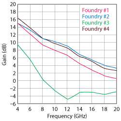
Figure 1 GaN devices from four foundries, comparing small-signal gain vs. frequency.
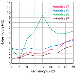
Figure 2 GaN devices from four foundries, comparing noise figure vs. frequency.
The MHEMT devices are much more susceptible to high input power levels than standard GaAs, since MHEMT achieves a lower noise figure in part by reducing the breakdown voltage of the device. Thus, the input limiter takes on an even more critical role within a receiver utilizing MHEMT technology.
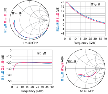
Figure 3 Comparison of measured (blue) and extracted model (red) S-parameters for a 4 × 100 µm GaN FET from Foundry #4.
The need for a limiter led Custom MMIC to consider an alternate solution to the problem of receiver sensitivity in high power environments. Through a Phase I and Phase II Small Business Innovative Research (SBIR) grant with the United States Air Force, Custom MMIC investigated the use of gallium nitride (GaN) technology for the development of the LNA. When GaN is raised as a topic in conversation, most engineers immediately think of power amplification, since the technology’s impressive breakdown voltage can be used to generate high power with high efficiency across the microwave spectrum. Such applications are not the only use for GaN. As circuit designers are discovering, GaN, with its high breakdown voltage, offers numerous advantages in other circuit functions, including LNAs.3-5
Custom MMIC embarked on an investigation of GaN as a replacement for GaAs LNAs in X and Ku-Band by exploring two key questions: Is the noise figure of a GaN device similar to a GaAs HEMT device? Can a GaN LNA survive incident power levels up to 5 W, thereby negating the need for an external limiter? The answer to both questions is a resounding “yes!”
GaN SELECTION AND MODELING
The first step in answering these questions was to identify a commercial GaN foundry with a low noise device that could support the required X to Ku-Band frequency range. Custom MMIC procured devices of roughly the same total periphery from four commercial foundries and measured their inherent gain and noise properties (see Figures 1 and 2). For these measurements, all of the devices were measured in a 50 ohm environment, biased with a drain voltage of 10 V and tuned to a current density of 250 mA per mm. Based on these results, Foundry #4 was the best overall choice, since it offered the lowest noise figure while still maintaining adequate gain. This foundry offers a GaN process with a 0.2 µm gate length, two levels of metal interconnects, metal-insulator-metal capacitors, airbridges, backside vias and a substrate thickness of 4 mils.
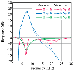
Figure 4 Comparison of the magnitude of the S-parameters vs. frequency, showing the measured (dashed lines) and the circuit model (solid lines) of an earlier, narrow-band version of the X-Band LNA.
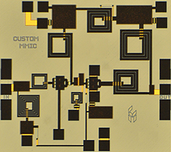
Figure 5 X-Band GaN LNA die fabricated by Foundry #4.
After choosing the foundry, the next step was to develop a scalable, small-signal GaN device model. Custom MMIC accomplished this by first measuring the Y-parameters for different device sizes under a range of bias conditions, then fitting these results to a standard FET circuit model. Figure 3 shows a comparison of the measured data for a 4 × 100 µm device against the extracted circuit model, where Vdd = 10 V and Vgg = -2.8 V. Note that the model predicts the gain of the device to within 0.75 dB up through 40 GHz. It achieved a similar level of modeling accuracy across a wide range of device sizes and bias conditions.
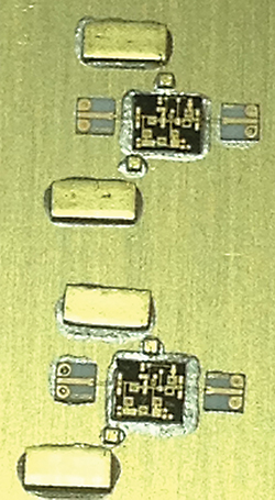
Figure 6 Die plate assembly for testing the GaN LNA with bond wire interconnects.
Of course, the device model by itself is not the complete story, the authors are most concerned with accurately simulating the entire LNA. Figure 4 shows a comparison of the measured data with the circuit model for an early iteration X-Band LNA design. This amplifier was designed to operate near 7 GHz with a relatively narrow bandwidth, which makes this circuit ideal for comparing the model and the measured data. The model predicts the S-parameters with very good accuracy, including the resonant nulls in the port return losses. Its device models have been used to design narrowband and wideband amplifiers to 20 GHz, all with the same success as shown in Figure 4.
GaN LNA DESIGN
Once Custom MMIC had developed GaN models and examined preliminary designs, they focused on developing an ultra low noise GaN amplifier covering 5 to 9 GHz. They settled on a two-stage topology with highpass matching networks for the input and interstage. Highpass networks tamp down the low frequency gain, ensure unconditional stability and provide a good noise match. Figure 5 is a photograph of the die as manufactured. The input is on the left, the output on the right; drain voltage is applied at the top, gate voltage at the bottom. All grounds are accessed through backside vias. The bright gold traces show the bottom metal layer, the dark traces represent the upper (airbridged) metal layer. This design does not include a front-end limiter.
For testing, Custom MMIC mounted the die to a metal carrier and attached bypass capacitors to the bias ports with bond wires. Figure 6 shows a photograph of the plate assembly. The LNA was biased with a fixed drain voltage (Vdd) of 10 V and a variable gate voltage (Vgg) between -2.4 and -2.8 V, corresponding to a quiescent current between 60 and 150 mA. The bias was connected to the LNA through needle probes to the top plate of the bypass capacitors. The input and output ports were bonded to 50 ohm alumina microstrip lines that were accessed with standard ground-signal-ground wafer probes. All measurements included the presence of bond wires. High performance microwave cables connected the wafer probes to the test equipment. Calibration was performed to the ends of the wafer probes for both vector (S-parameter) and scalar (noise figure) measurements.
Figure 7 shows the magnitude of the measured S-parameters. The drain voltage was 10 V, and the gate bias varied from -2.4 to -2.8 V. The gain of the LNA was between 20 and 24 dB, with return losses better than -10 dB across 6 to 8 GHz. These parameters are fairly insensitive to the gate bias. Figure 8 shows the noise figure of the LNA under the same bias conditions used for measuring the S-parameters. The noise figure is 1.0 to 1.3 dB across 5 to 9 GHz, with an optimal gate bias, approximately Vgg = -2.6 V. The output power at 1 dB compression and third order intercept are plotted in Figure 9. The LNA had a fixed gate bias of Vgg = -2.6 V and a drain bias of Vdd = 10 V. The LNA delivers a fair amount of power and reaches a peak power-added-efficiency (PAE) of approximately 30 percent under drive. Such efficiency is noticeably better than most typical GaAs LNA designs, which tend to have a PAE on the order of 10 percent.
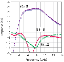
Figure 7 Magnitude of the S-parameters of the GaN LNA vs. frequency, biased at gate voltages between –2.8 and –2.4 V with Vdd = 10 V.
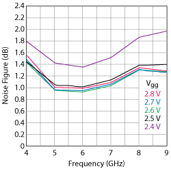
Figure 8 Noise figure of the GaN LNA vs. frequency, biased at gate voltages between –2.8 and –2.4 V with Vdd = 10 V. The optimal gate bias is –2.6 V.
The noise performance of this GaN LNA is commensurate with a GaAs HEMT design.6 However, the GaN amplifier delivers much more power with greater efficiency, generating a much wider dynamic range than its GaAs counterpart.
DAMAGE TESTING
The second goal of this effort was to investigate the ability of a GaN LNA to withstand high incident power. Numerous other researchers have considered this problem3,7 and demonstrated GaN LNA survivability levels at X-Band ranging from +32 to +42 dBm. However, nearly all of the LNAs capable of surviving above +38 dBm have bandwidths much less than the near octave bandwidth of Custom MMIC’s design. Therefore, the authors believe their work advances the overall knowledge of GaN LNA robustness.
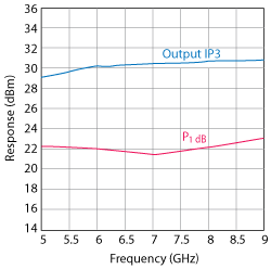
Figure 9 Output power at 1 dB compression and output IP3 vs. frequency for the GaN LNA biased at Vdd = 10 V and Vgg = –2.6 V.
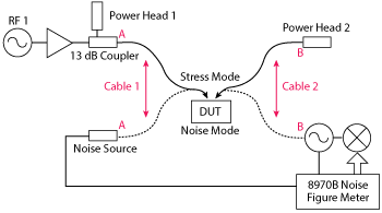
Figure 10 Setup for high power stress testing the GaN LNA.
To investigate power handling, they developed a scalar test station (see Figure 10) that stresses the input port of the LNA up to incident power levels of 5 W and then measures the gain and noise figure of the amplifier. In the stress mode, the device-under-test (DUT) was subjected to a high power signal for ten seconds. The power was calibrated using scalar power detectors (power heads 1 and 2 in Figure 10). The test sequence began at 1 W incident power and increased to 5 W, the maximum input power available from the equipment. After each 10 second stressing, the LNA was connected to the measurement path (“noise mode” in Figure 10) and compared to the baseline gain, noise figure and DC current.
Figures 11 and 12 show the measured gain and noise figure, respectively, after a number of stress tests. Both parameters remained relatively unchanged until the LNA was subjected to 5 W of incident power, when the gain dropped approximately 0.4 to 1 dB, and the noise figure rose by 0.2 dB. Following this final stress test, the LNA remained biased with no RF drive for five minutes; then the parameters were retested. Both gain and noise figure recovered to within their normal limits after this settling period. Therefore, the authors believe they have demonstrated an LNA that survives incident power levels up to 5 W without suffering long-term damage.
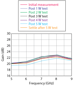
Figure 11 Gain of the GaN LNA before and after stress testing, biased at Vdd = 10 V and Vgg = –2.6 V.
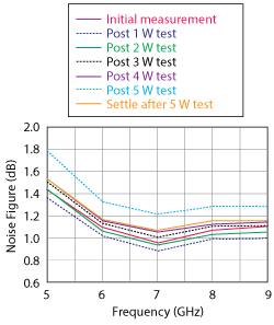
Figure 12 Noise figure of the GaN LNA before and after stress testing, biased at Vdd = 10 V and Vgg = –2.6 V.
This same power handling investigation was performed on several other X-Band LNA designs with similar noise figure but reduced output power. The lower power was achieved by using smaller GaN devices in the same amplifier topology (two-stage with highpass matching networks), not by varying the bias point of the baseline design. The smaller the device, the less input power the LNA could withstand before damage. For example, an LNA with 50 percent less periphery than the original design could only withstand incident levels up to 2 W; an LNA with 75 percent less periphery could only withstand levels of 1 W. There does appear to be a direct correlation between GaN device size and inherent overdrive protection.
CONCLUSION
The authors have demonstrated an X-Band LNA fabricated on a commercial GaN process with an ultra-low noise figure of 1.0 to 1.3 dB. This LNA was a two-stage design that utilized highpass matching structures in the input and interstage networks. Without an input limiter, the LNA was able to withstand incident power levels of 5 W for 10 seconds without suffering long-term damage. Survivability in such an environment appears directly related to the device size within the LNA, at least for a fixed topology.
ACKNOWLEDGMENTS
This work was partially funded by the Sensors Directorate, Air Force Research Laboratory, Wright-Patterson Air Force Base, under an SBIR grant contract number FA8650-12-C-1355. Custom MMIC would like to thank the United States Air Force for their encouragement of this work throughout the research program.
References
- P. Blount, “X-Band and Ka-Band Low-Noise Block Downconverter,” final report AFRL-RY-WP-TR-2014-0181, Air Force Research Laboratory, Wright-Patterson AFB, September 2014.
- P. Blount et al., “Low Noise, Low Power Dissipation mHEMT-based Amplifiers for Phased Array Applications,” IEEE International Symposium on Phased Array Systems and Technology Digest, pp. 233–237, October 2010.
- S. Colangeli et al., “GaN-Based Robust Low-Noise-Amplifiers,” IEEE Transactions Electron Dev.,Vol. 60, No. 10, pp. 3238–3248, October 2013.
- D. Resca et al., “A Robust Ku-Band Low Noise Amplifier Using an Industrial 0.25-um AlGaN/GaN on SiC Process,” European Microwave Integrated Circ. Conf. (EuMIC), pp. 496–499, October 2013.
- W. Chang et al., “X-Band Low Noise amplifier MMIC Using AlGaN/GaN HEMT Technology on SiC Substrate,” Asia-Pacific Microwave Conference Proceedings (APMC), pp. 681–684, November 2013.
- Data sheet for the CMD119P3, www.custommmic.com/Product-Library/Amplifiers/.
- M. Rudolph, “Highly Rugged and Highly Linear GaN LNAs,”IEEE International Microwave Symposium Digest, Workshop WMD-7, pp. 183–223, June 2014.