
Active electronically scanned array (AESA) antennas have been employed for military phased array radar systems for over five decades. Their popularity has dramatically increased recently as advances in technology enable compact, low cost arrays for commercial applications.1 As they are adopted for markets as disparate as weather radar, sense-and-avoid radar for commercial and private drones, global ground-satellite communication for Internet access as well as 5G infrastructure, they are poised to become even more prevalent.2 Indeed, the use of phased array techniques to provide advanced antenna aperture capabilities is seen as fundamental to the rollout of 5G infrastructure.3,4
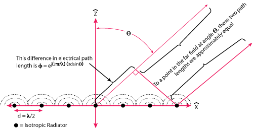
Figure 1 Simplified one-dimensional planar array antenna consisting of a row of isotropic radiators. The far field antenna pattern is a composite of the excitations at each element.
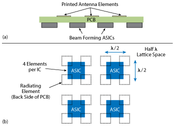
Figure 2 Side (a) and plan (b) views, showing beam forming ASICs mounted on the backside of the planar antenna array.
One of the driving technologies for this path to growing adoption is the increasing use of silicon-based (Si) technologies (SiGe BiCMOS and RF CMOS) to provide increased functional density and capability within a single die/package.5 This article reviews some of the technical challenges of building high density planar phased arrays and suggests that solutions to these problems can be found by greatly increasing the level of integration in the IC solutions, thus enabling large-scale planar AESA arrays. By taking advantage of the integration capability of silicon, additional system level functionality such as on-chip diagnostics, built-in self-test (BIST) and built-in calibration
(BICAL) can be utilized to give the end user far more visibility and control over the operation of the array. Examples of the performance features that can be embedded into highly integrated application specific integrated circuits (ASIC) used in silicon-based AESA arrays will be discussed.
Figure 1 shows a simplified one-dimensional illustration of a phased array antenna, consisting of a row of isotropic radiators. The composite response of the antenna pattern in the far-field is a function of the amplitude and phase excitation at each element. Simplistically, the careful control of each amplitude and phase response determines the magnitude and scan angle of a single- or multi-beam antenna pattern. One of the constraints for a wide scan angle antenna pattern is the restriction that each of the antenna elements is spaced by no more than a free space half wavelength (λ0) to avoid the generation of grating lobes, where waves from each element are summed in phase producing beams in undesired directions.6,7 Beamforming can be performed in either the analog or the digital domain (or both) with trade-offs in system performance for complexity, linearity and power dissipation.
Planar phased array antenna solutions are attractive in providing a compact, and potentially low-profile form, thus enabling their use in a broader range of applications.2 The primary enabler for a planar-form solution is for the analog beamforming circuitry – transmit (Tx), receive (Rx) or transceiver (Xcvr) – to fit physically between the elements of the antenna lattice. Figure 2 shows an illustration of how this may be realized, where the beamforming ASICs are surface mounted to a PCB with the antenna radiating surface on the opposite side. Note that in this highly idealized drawing, signal routing and heat sinks for thermal power management are not shown.
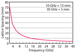
Figure 3 Half wavelength lattice spacing vs. frequency.
So far, so good. But the challenge of this approach can be appreciated by considering how the available physical dimensions rapidly shrink as a function of frequency. To a first order, the lattice spacing between antenna elements is constrained to a half wavelength to avoid the presence of grating lobes, which is plotted in Figure 3 as a function of the operating frequency. (In reality, the maximum spacing is also a function of the maximum required scan angle). The physical constraints governing the available area for component integration falls dramatically from 37.5 mm at 4 GHz (S-Band) to 15 mm at 10 GHz (X-Band) and only 5 mm at 30 GHz (Ka-Band).
Unfortunately, discrete based solutions in commercially available surface mount device (SMD) packages can easily exceed these limitations, as their combined area and allowance for interconnects and support componentry occupy a large footprint. At X-Band and above, increased integration becomes the only way to make such a planar system a viable option. Solutions have become available in recent years that integrate single element beam formers with Tx/Rx functionality in a single package.8 GaAs technologies that are commonly used for these functions due to their high electron mobility and associated performance metrics are expensive and limited in their integration capability. By comparison, high performance SiGe BiCMOS and RF CMOS have demonstrated the required performance at microwave and millimeter wave frequencies in multiple applications.5 In addition, their ability to integrate dense functionality results in the potential for combining product solutions that can support multiple radiating elements within a single package. Figure 4 is a functional block diagram of a single component that simultaneously supports dual polarization and four radiating elements.
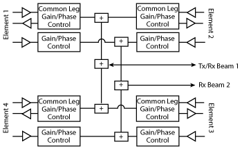
Figure 4 Functional block diagram of the integrated TDD T/R chip.
Highly Integrated Solution
This section reviews an example of how a highly integrated TDD (time-domain duplex) transmit-receive chip supporting four discrete antenna elements may be configured to meet the objective requirements of cost, size and functionality. It is packaged within a standard commercial QFN-style plastic package measuring 7 × 7 × 0.9 mm, and easily fits within the 15 mm lattice spacing at 10 GHz for X-Band applications. The IC consists of four distinct quadrants that can each be operated and controlled discretely, with the ability to simultaneously drive four antenna elements in transmit mode. In addition, there are eight independent receive ports – two per quadrant – that allow for dual polarization on each antenna element when operating in receive mode. Transmit and receive waveforms can be weighted independently with 12-bit complex vector modulators consisting of 6-bit phase control, where the least significant bit (LSB) is 5.625 degrees, and 6-bit amplitude control, providing 31.5 dB dynamic range and LSB of 0.5 dB.
Figure 4 shows this partitioning in more detail. Each quadrant consists of a Tx/Rx arm sharing a common path vector modulator (complex amplitude and phase) as well as a second receive-only arm which shadows the Tx/Rx function. Central to the quadrant based operation is a chip-core where the modulated received signals are coherently combined and feed a common RF port. The TDD based operation of the die allows the combiner network of the Tx/Rx arm to be used for coherent power splitting when operating in the transmit mode. Over 31 dB of dynamic range is therefore available in each discrete antenna element path through varying the discrete vector modulators. This dynamic range can be used for array taper or other gain control functions. The settings of each of the vector modulators, as well as the other functions on the chip, are controlled using a serial peripheral interface (SPI) for data transfer and control signal management.
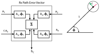
Figure 5 Unwanted signal coupling degrades modulated waveform accuracy, inducing AM-AM and AM-PM errors.
Temperature compensation of the entire chip can be enabled through additional digital variable attenuators (DVA), allied with active gain stages in each of the common combiner ports to extend the controllable dynamic range of the IC to over 50 dB. This can be used in conjunction with an on-chip temperature sensor to account for temperature changes within the IC and also compensate other temperature sensitive components elsewhere in the system. Real-time, closed loop temperature compensation can be implemented by reading data from the IC temperature sensor, updating the appropriate settings and using available data for external components. Maximum system flexibility results from the gain control partitioning provided by the chip.
Phase and Amplitude Accuracy
Although an increase in the number of antenna elements that can be supported by a single component, by utilizing the benefits of the functional integration density of Si, has several advantages (i.e., reduced bill-of-materials, reduced inventory, smaller PCB integration form-factor), it is not an approach that can be followed with impunity. Other functional and performance considerations include the ease of routing low-loss and controlled impedance transitions between the various RF ports and the antenna elements, thermal dissipation paths, the number of external components, signal and supply path constraints and unwanted signal coupling.
Figure 5 shows how signal coupling and appropriate isolation between signal paths needs to be considered and the potential limitations they may impose on system performance. In this example, four discrete Rx paths – a1, a2, a3, and a4 – are input to a common beamformer IC and coherently combined with a summed output signal of bc. Ideally, each of the four signal paths would remain isolated up to the input of the summing network, and the complex beam weight (Ai, Φi) applied to each signal would have zero associated amplitude and phase error. In reality, non-idealities in each of the vector modulators and other components in each signal path will impose some level of AM-AM, PM-AM and AM-PM distortion, resulting in an associated error in the signal vector. In theory, any of these corrupting influences are well known and modeled during the design phase; as long as they are maintained below the magnitude of ½ LSB, they should not degrade performance.
More difficult to deal with is coupling between signal paths that may be less predictable, arising from several sources including signal transmission lines between the antenna elements and the component RF ports, signal coupling within the package through the unwanted radiation of bondwire transitions, dielectric material loading of the package over-mold and parasitic and leakage path coupling through other on-chip networks that are more difficult to account for at high frequencies.9 These may include such disparate paths as bias distribution networks, pad-rings and ESD domain coupling. Regardless of the source, the effect illustrated in Figure 5 produces the same result: distortion of the desired vector by a parasitic phasor that causes amplitude or phase distortion or both. In the simplest case, maximum amplitude error occurs when the coupled phasor is in phase with or exactly out of phase with the desired vector. Here, the magnitude of the error vector is

Similarly, the maximum phase error occurs when the coupled phasor is orthogonal to the phase of the desired vector, resulting in a maximum phase error of
The magnitude of the total amplitude and phase error of the desired vector needs to be maintained below ½ LSB, leading to a relationship between the number of available bits of amplitude and phase resolution and the allowable level of coupling between signal paths. Figure 6 shows how this relationship varies for several combinations of vector modulator resolution. For example, to maintain the required accuracy for 6-bit amplitude and phase control, the magnitude of the worst case error vector needs to be less than 26 dB when normalized to a vector magnitude of 1. This figure, though, does not account for the effect of channel gain on the magnitude of the coupled signal. Figure 7 shows how the level of coherent gain imposes more stringent requirements on the allowable coupling and drives increased channel-channel isolation. As the desired channel gain increases, the required coupling must decrease dB for dB to keep the same ½ LSB error. For example, if the channel gain is 20 dB and the vector modulator provides 6-bit complex modulation, the absolute isolation required becomes 26 dB + 20 dB or 46 dB.
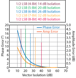
Figure 6 Phase and amplitude error vs. coupled path isolation.
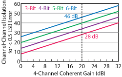
Figure 7 Required minimum channel-channel isolation increases with coherent gain.
Actual Performance Metrics
This section presents measured data for a commercially available 4-element beam former IC, to indicate the available performance for a highly integrated, multi-element solution. Figure 8 shows the measured coherent receiver gain, which is defined as the combined (superimposed) signal gain between each of the four receiver ports and the output of the coherent combiner. The vector modulator for each signal path is set to a common complex beam weight for this measurement, resulting in a coherent gain that is approximately 7 dB across the band. The amplitude imbalance between the ports is < 1 dB, including mismatch. Noise figure (NF) versus frequency is shown in Figure 9. This has been adjusted to reflect the NF seen when each port is driven from non-coherent noise sources. The NF at the center of the band is 14 dB. If only a single channel were measured, the resulting NF would be 4.1 dB higher. The input 1 dB compression point for the receiver is approximately -2 dBm at the center of the band. This is measured on a single channel.
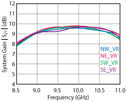
Figure 8 Measured coherent receiver gain, showing < 1 dB imbalance across four channels.
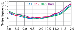
Figure 9 Measured receiver noise figure. The four channels are assumed to be driven by non-coherent noise sources.
The performance of the vector modulator is shown in Figure 10. All 12 bits of amplitude and phase states (4,096 states) were measured and graphed on a polar plot. The concentric circles and linear spokes of the figure are indicative of the low PM-AM and AM-PM distortion of the vector modulator. Figure 11 shows the explicit RMS phase and amplitude error across the band. The amplitude error is less than 0.5 dB, while the phase error is less than 3 degrees, or about 2/3 LSB. The channel-channel isolation can be inferred from a combination of measured S-parameters and beam rotation. A signal coupled to the common output port and superimposed upon the desired signal vector will cause AM-AM and AM-PM errors in the signal vector, as previously described. By measuring the signal path from any Rx input to the common output beam former port and adjusting the beam weight settings of the non-signal path vector modulators, the magnitude of the signal coupling into the main signal path can be estimated, as shown figuratively in Figure 5. The measured error in the phase response is approximately ±1.5 degrees as shown in Figure 12, corresponding to a port-port isolation of approximately -38 dB, accounting for the coherent receiver gain.
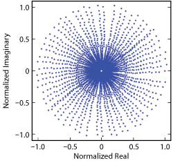
Figure 10 Measured 12-bit vector modulator (6-bit amplitude and 6-bit phase) state map at 9.4 GHz.
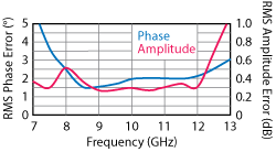
Figure 11 Measured RMS amplitude and phase error across X-Band.
Advanced Features with Integration
The core technology enabler of dense functional integration is the ability to integrate multiple controllable circuit blocks within a single die using Si-based processes and control the operation using the SPI ports. It is then only a small additional step to use the access to the die provided by the SPI to embed supplementary functions and controls that can be controlled digitally by the customer to increase operational flexibility. In this example, a proprietary 5-wire, 50 MHz SPI has been used. This has been designed to minimize coupling between digital and RF signals. With the proprietary SPI bus, multiple ICs in a row or column or any other subset of an array can be daisy chained and driven by a single bus and latched in tandem.
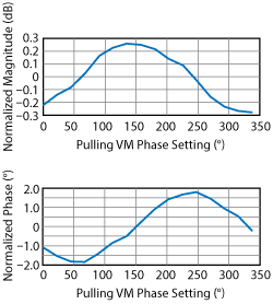
Figure 12 Signal magnitude and phase error from unwanted signal coupling to adjacent ports.
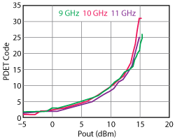
Figure 13 Transmit path output power code vs. input power at 9, 10 and 11 GHz.
In addition to the ability to write vectors to multiple registers, the SPI also allows read-back from functional blocks on the IC. This capability gives the array system integrator insight into real-time operation through the addition of on-chip telemetry. Each transmit arm includes an on-chip power detector that samples the output signal with 5-bit resolution and provides the power measurement as a digital word to the SPI. In addition, the time at which the transmit power is measured can be determined by the user. This accommodates radar systems with varying pulse widths and also provides information on transmit pulse droop, if the measurement interval is varied pulse to pulse. Figure 13 shows the detector output vs. power level and frequency. Similarly, on-chip temperature sensing provides real-time information and insight into the reliability of the IC.
Separate pins are provided to enable either transmit or receive mode, providing the flexibility to select the desired set-up time between activating transmit or receive DC power and when the RF waveform is applied. To minimize power dissipation, all transmit functions are powered down when the IC is in receive mode and vice-versa during transmit. The DC power consumption is 1.8 W in transmit, 1.7 W in receive if both receive beams (4-elements, dual polarization) are active and 1.3 W in receive if only one receive beam (4-elements, single polarization) is active. The chip is biased with a 1.8 V supply.
Another feature is the ability to set the chip in a calibration mode, where only one quadrant at a time is enabled. Separate pins are provided to communicate with an external front-end chip so that a complete channel-by-channel calibration can be performed. A further programming feature is the delay time between data latch and beam weight adjustment. The simultaneous change to all of the transmitters in a large array can create spurious lobes and system level problems. Dithering the time between latch and change for each IC can avoid this.
Lastly, programming the vector modulator for a single IC only takes 4.5 µs at 50 MHz. If a large number of ICs are daisy-chained for row-column addressing operations, the entire process can take substantially longer. One solution to this is to allow fast beam steering (FBS) by incorporating a programmable register stack with each vector modulator that can be pre-programmed with 12 bits of phase and amplitude information. Each vector modulator has a stack of eight registers that can be pre-loaded using the SPI bus and then directly addressed via a 3-bit direct addressing parallel interface, eliminating the wait for a serial load via the SPI bus. This means that the beams can be switched in as fast as 50 ns. These two modes, programming on the fly and fast beam steering, provide flexibility for any radar application.
Conclusion
Planar AESAs require increased compaction of circuit functionality to maintain the required form factors at high frequencies. This is driven by the minimum lattice spacing requirements of antenna elements, to avoid the introduction of grating lobes in the radiation patterns of the antenna. One of the consequences of increased functional density is reducing the number of required components and reducing the cost for the entire bill-of-materials. A proven method for achieving this compaction is realizing the circuitry in a highly integrated Si IC. Additional benefits of this technology are the ability to integrate control and tuning elements to trim the optimal performance of the IC, using a serial interface, and providing telemetry for system monitoring, such as temperature and output power. Reducing the physical dimensions requires careful design to avoid limiting the accuracy of the available beam weight resolution through unwanted signal coupling paths; however, this has been shown to be possible. Other performance metrics possible with a 12-port IC supporting dual-polarization Tx/Rx receive functionality for a 4-element antenna solution have also been presented.
Acknowledgment
The authors thank the entire staff of Anokiwave for their ideas, enthusiasm and contributions to this work.
References
- E. Brookner, “Phased-array Radars: Past, Astounding Breakthroughs and Future Trends,” Microwave Journal, January 2008.
- G. Fields,“Phased-array Radar at The Intersection of Military and Commercial Innovation,” Microwave Journal, January 2014.
- T. Rappaport et al., “Millimeter Wave Wirelesss Communications,”Prentice-Hall, 2015.
- “IBM and Ericsson Collaborate on 5G Antenna Designs,”Ericsson press release, November 24, 2014.
- G. Rebeiz et al.,“Millimeter-Wave Large-Scale Phased-Arrays for 5G Systems,”IEEE MTT-S International Microwave Symposium, 2015.
- R. C. Hansen,“Phased Array Antennas,”John Wiley & Sons, 1998.
- A. J. Fenn et al.,“The Development of Phased-Array Radar Technology,” MIT Lincoln Laboratory Journal, Vol. 12, No. 2, 2000.
- D. Heo et al., “Integrated Eight Element Ku-Band Transmit/receive Beamformer Chipset for Low-cost Commercial Phased Array Antennas,”IEEE International Symposium on Phased Array Systems and Technology, October 2010.
- G. Rebeiz,“Effect of Output-to-Input Coupling on Phased Arrays,”Personal Communication, May 2014.
Ian Gresham is a technology fellow at Anokiwave, where he serves as IC system architect. Gresham has over 25 years experience in radar, telecommunications and semiconductor technology and has contributed to the product and technology development at NXP and M/A-COM. He holds bachelor’s and doctorate degrees from the University of Leeds and is a fellow of the IEEE.
Rob McMorrow has over 20 years experience in RF circuit design, particularly power amplifiers. Before joining Anokiwave, he was co-founder and chief technical officer of Star RF/Xikota Devices, formed to develop CMOS PAs for wireless handsets. His design expertise has also served Raytheon, Skyworks and Analog Devices. McMorrow received his bachelor’s and master’s degrees from Cornell University.
David Corman is chief systems architect at Anokiwave, applying his 34 years experience in RF system, module and RFIC/MMIC design. Previously, he co-founded US Monolithics and spent 15 years at Motorola. At Motorola, he was the architect and lead technologist for the Iridium Block 1 space-based K- and Ka-Band electronics suite. His contributions have been recognized with over 40 patents. Corman received his bachelor’s degree from the University of Kansas and a master’s from Arizona State University.
Nitin Jain founded Anokiwave in 2000, where he designs and consults with customers. Before starting Anokiwave, he was at M/A-COM, where his contributions included leading the technical development of a 77 GHz automotive radar module. Jain has been awarded 20 U.S. patents and has written more than 37 papers and articles. He holds a bachelor’s degree from the Indian Institute of Technology and master’s and doctorate degrees from Rensselaer Polytechnic Institute.