
The growing usage of multimedia applications associated with consumers’ desire for the ultimate mobility experience have propelled the smartphone IC device segment into the largest semiconductor market. Smartphone front-end modules (FEM), the interface between the phone and the external world as depicted in Figure 1, is a key function of the mobile phone, and its design directly impacts the cellular network and critical handset performances: range, data rate, sound quality and battery life.1 The FEM economic value and board footprint are comparable to phone processor and memory, making it a major focus of the phone industry.
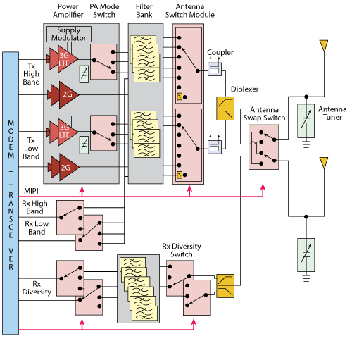
Figure 1 FEM block diagram.
FEMs are made up of many different functions such as filters, switches, power amplifiers, low noise amplifiers, couplers, duplexers, antenna tuners and antennas. The number and requirements of those functions increase with the number of bands the smartphone needs to support. Each one of these functions inside the FEM requires a specific engineered substrate to meet the optimal cost and performance target of the system. For example, as mainstream technologies, filters are based on piezoelectric materials: aluminium nitride (AlN), lithium tantalate (LiTaO3) and lithium niobate (LiNbO3). Power amplifiers are based on gallium arsenide (GaAs), switches are based on high resistive silicon on insulator (HR SOI) and antenna and FEM assemblies rely on advanced polymers, ceramics and metal materials structures.
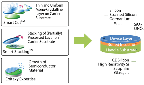
Figure 2 Engineering substrate toolbox.
Engineered Substrate Tool Box
Engineered substrates are designed based on a generic tool box as illustrated in Figure 2. The first tool, called Smart Cut™ technology, enables transfer to a thin (from few 10s of nm to 2 µm) and uniform mono-crystalline layer on a carrier substrate. The second tool called Smart Stacking™ technology enables stacking of partially or fully processed layers on a carrier substrate. The third tool, epitaxy, is a technology used to grow a semiconductor material on a carrier substrate. With this tool box, engineered substrates that are designed are typically made of three layers. The top layer is dedicated to the implementation of the electronic devices (transistor, passive components, etc.), the intermediate layer, an isolation interface usually made of an oxide called buried oxide (BOX) and the bottom layer which provides the mechanical support of the structure, usually called a handle substrate. It is important to note that those layers may also have some impact on characteristics such as thermal dissipation, reflection properties and signal attenuation, and they need to be carefully chosen and designed.
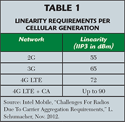
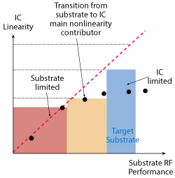
Figure 3 IC linearity vs. substrate RF performance.
Linearity Challenge
According to Cisco,2 mobile data traffic will grow at a 61 percent CAGR between 2013 and 2018, mainly driven by multimedia applications and, in particular, video exchange. The cellular roadmap is addressing this data traffic boom by improving spectral efficiency, increasing available spectrum and increasing network cell density. Key techniques to increase capacity are carrier aggregation and MIMO (multi-input-multi-output). To be efficient, those transmission techniques impose additional requirements on the FEM such as higher linearity, as shown in Table 1.
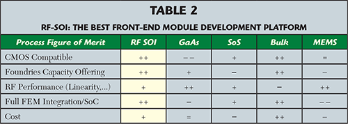
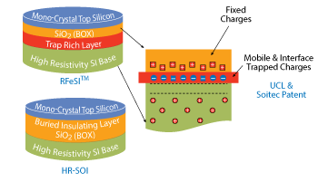
Figure 4 Types of RF SOI: HR-SOI and RFeSI™.
The entire ecosystem, from FEM makers, foundries, substrate suppliers and research centers, is working together to achieve those linearity requirements. Engineered substrate providers are trying to provide substrates that will enable better RF performance and not become the limiting factor for the device. Figure 3 shows the contributions to linearity.
RF SOI Substrates
Depending on the architecture and partitioning of the FEM, device linearity requirements may change drastically from one component to the other. As a rule of thumb, the devices closer to the antenna or the devices on the path of stronger signals will need to exhibit higher linearity. RF SOI is an engineered substrate which comprises a thin film of mono crystalline silicon fully CMOS compatible as the top layer, an oxide as the isolation layer and a high resistive substrate as the handle substrate. The substrate resistivity can be several kΩ-cm and should be as high as 10 kΩ-cm to be considered as RF lossless. As shown in Table 2, RF SOI offers a global design platform for FEMs with several advantages compared to other available options (CMOS compatibility, foundry offering, RF performance, integration and cost effectiveness).
RF SOI includes two different type of substrates: standard high resistive SOI (HR SOI) and enhanced signal integrity SOI (RFeSI™ SOI). In the RF SOI products, the oxide of the insulator BOX still contains positive charges in the range of a few 10E10 cm2. As demonstrated by Prof. Raskin’s work from Université Catholique of Louvain (UCL), those charges create a parasitic surface conduction at the interface between the BOX and the high-resistivity handle substrate, typically dropping its resistivity by a decade.3,4 To recover the original resistivity of the handle substrate, UCL and Soitec have invented a method consisting of adding a trap-rich layer on top of the handle wafer that can freeze those carriers as shown in Figure 4. Depending on the linearity requirements, designers have then the option to choose one or the other substrate depending on the level of RF performance required for their application; they could even use the same design, optimizing the best cost performance trade-off.
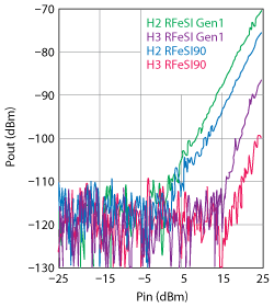
Figure 5 Second (H2) and third (H3) harmonics measured on RFeSI Gen1 and RFeSI90.
UCL and Soitec have widely published comparisons between bulk Si, HR SOI, RFeSI and quartz substrates.5,6,7 As a summary, the RFeSI substrate addresses the critical FEM requirements: higher linearity, reduced crosstalk, lower insertion loss, better passive device quality factor and, to some extent, higher thermal dissipation. RF SOI substrates have become the mainstream substrate for switches with more than 85 percent market share in antenna switch modules.8 After a few years of production of the first generation RFeSI substrate, a second generation (called RFeSI90 substrate) has been introduced this year in order to keep up with increasing market linearity requirements. As shown in Figures 5 and 6, RFeSI90 substrates offer 10 dB better linearity than RFeSI Gen1 substrates. This makes it suitable for the most advanced circuits in new LTE-A smartphone applications, while RFeSI Gen1 continues to serve the current market. Improvements have been achieved using a combination of increased handle substrate resistivity as well as a re-engineering of the trap-rich layer. The BOX thickness has also been reduced by a factor of two without impacting the RF device performance while improving manufacturability.
RF metrology – Harmonic Quality Factor
As shown in Figure 7, there is a gap between the substrate world where we talk about contaminant, oxygen level, dopant, layer thickness and more material-oriented concepts and the RF designer’s world more concerned about RF linearity, losses, power dissipation and IC design-oriented concepts. Bridging this gap between the engineered substrate specifications and the IC linearity specification is a concern for all foundries and RFIC designers when choosing an RF engineered substrate.
Materials engineering and RF engineering are two different domains, and specifying the resistivity of the handle substrate using an ohmic sheet resistance measurement at the backside of the substrate will not guarantee the RF performance of the wafer. There are many parameters that can change the RF performance of an RFeSI wafer: the trap-rich layer material and its characteristics, dopants that can migrate at interfaces between the layers, activation of thermal donors during the Smart Cut and foundry process temperature cycles, doping profile and thickness of the different layers, etc. To measure resistivity across the wafer, a technique called spreading resistance profile (SRP) is commonly used. To quantify the level of linearity of the material, manufacturers have traditionally measured the level of harmonics generated by a signal injected on a coplanar waveguide (CPW). Soitec has developed a proprietary algorithm which integrates the SRP profile weighted by the depth of the electrical field and matches it to the second harmonic generated through a CPW as shown on Figure 8. This parameter is called harmonic quality factor (HQF) and is included in the RFeSI substrate specifications.
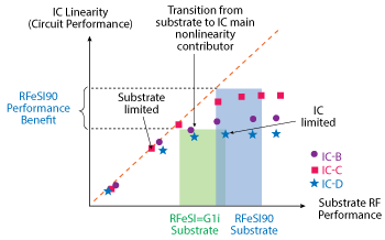
Figure 6 Linearity performance benefit depends on IC type and RFeSI substrate.
Beyond RF SOI Switches
Integrating more FEM devices is an on-going challenge for the industry. RF SOI is the ideal platform to expand this roadmap. RF SOI is already a mainstream technology for switches used in all different configurations (antenna, antenna swapping, power amplifier mode, diversity, antenna tuner). Active components such as LNAs and passive components such as couplers are also being integrated on a single die with switches. Power amplifiers using RF SOI were launched in the market in 2013 addressing the LTE and LTE-A market, chosen by some first adopters like ZTE. Tunable filter solutions partly or fully integrated on RF SOI are in research and development. The competition with current piezoelectric filters, having quality factors of few thousands, is difficult with typical discrete and on-chip inductors that have quality factors of a hundred or less. The first phase is to lower the filter bill of materials by doing part of the filtering on chip.
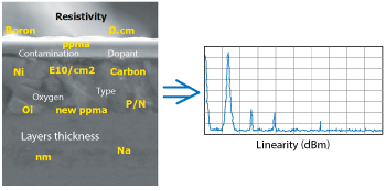
Figure 7 Improving RF performance requires understanding how wafer parameters affect linearity.
Some RF SOI foundries have begun offering 300 mm diameter wafers. We expect future offerings of process nodes beyond 90 nm that will provide opportunities to address applications beyond the current FEM technology by combining advanced digital processing and analog SOI advantages: faster frequency operation at the same node compared to bulk silicon, lower supply voltage operation down to 0.4 V, high voltage handling, temperature operation much beyond 150°C, very low sensitivity to soft error rate and more. Recent switch technology history has demonstrated that in the high volume, highly competitive consumer electronics market, a new technology can very rapidly displace the incumbent technology, GaAs in this case. The engineered substrate tool box is extremely powerful, enabling the manufacture of the most adapted substrate for a very dynamic ecosystem ready to adopt new substrates when performance and cost warrants.
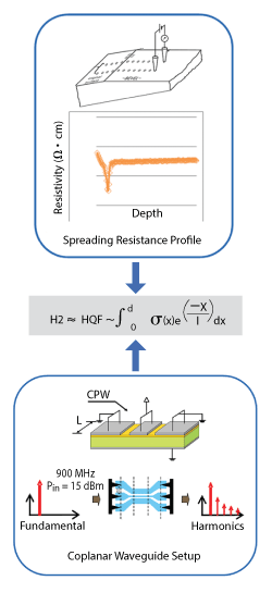
Figure 8 The HQF correlates the SRP with the measured second harmonic.
References
- E. Desbonnets, S. Laurent, “RF Substrate Technologies for Mobile Applications,” Soitec White Paper, 2011.
- Cisco VNI Mobile, February 2014
- D. Lederer and J.P. Raskin, “Effective Resistivity of Fully-Processed SOI Substrates,” Solid-State Electronics, Vol. 49, No. 3, 2005, pp. 4912496.
- D. Lederer and J.P. Raskin, “New Substrate Passivation Method Dedicated to HR SOI Wafer Fabrication with Increased Substrate Resistivity,” IEEE Electron Device Letters, Vol. 26, No. 11, 2005, pp. 8052807.
- K. Ben Ali, C. Roda Neve, A. Gharsallah, and J.P. Raskin, “RF Performance of SOI CMOS Technology on Commercial 200 mm High Resistivity Silicon Trap-Rich Wafers,” IEEE Transactions on Electron Devices, Vol. 61, No. 3, March 2014., pp. 7222728.
- C. Roda Neve and J.P. Raskin, “RF Harmonic Distortion of CPW Lines on HR-Si and Trap-Rich HR-Si Substrates,” IEEE Transactions on Electron Devices, Vol. 59, 2012, pp. 9242932.
- Yonghyun Shim, J.P. Raskin, C. Roda Neve and M. Rais-Zadeh, “RF MEMS Passives on High-Resistivity Silicon Substrates,” IEEE Microwave and Wireless Components Letters, Vol. 23, No. 12, December 2013, pp. 6322634.
- Sapphire Applications & Market: from LED to Consumer Electronic, Yole, 2014.