
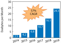
Figure 1 Global mobile data traffic forecast.2
RF SOI has taken the mobile RF world by storm recently in helping to solve the challenges that go along with ensuring users seamless, always available connectivity and access to the power of the Internet from virtually anywhere. The introduction of cloud computing is driving user expectations even higher. RF SOI is well positioned to become the innovation platform for delivering improved performance, lowering overall system costs needed to accommodate these rising expectations and staying ahead of the ever evolving network requirements. This article examines the industry trends that got us here, what’s next and how RF SOI can improve the performance of RF systems.
The Wireless Landscape
Rich content delivery to users has grown exponentially over the last five years. In developed countries, compressed high-definition video streaming over the Internet through services such as Netflix and Hulu is already nearly ubiquitous. The need for greater bandwidth will only increase as demands for higher quality content gives way to true uncompressed 1080p and 4K video delivery in the future. Cisco forecasts that by 2019, global Internet traffic will triple over 2014 levels, rising to 168 exabytes (EB) per month, a cumulative annual increase of over 23 percent.1
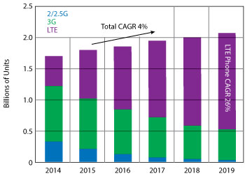
Figure 2 Global wireless handset forecast.3
The rise of cloud computing now allows this data rich content to be accessed anywhere and, more importantly, to be accessed anywhere while mobile. For an enhanced user experience, delivery of this content can be achieved only through higher data rates — within the confines of the available spectrum — with as low latency as possible. Demand for higher data rates is one of the main drivers for the evolution of current wireless communication standards. Over the last five years, both cellular and Wi-Fi have advanced at unprecedented rates. Cellular standards have transitioned from 2G/2.5G to 3G/4G, and now 4G/LTE. The same holds true for Wi-Fi standards, which have evolved from their humble 802.11a/b/g beginnings as a replacement for 56 Kbps wired modems to today’s 802.11ac, rivaling CAT6 wired Ethernet connections and promising wireless Gbps speeds.
Trends in mobile data consumption parallel this transition. Cisco also predicts that total global mobile data traffic will grow 10-fold between 2014 and 2019, to more than 24 EB per month (see Figure 1) — a growth rate nearly double that of global data traffic combined. To put this in perspective, this amount of data is equivalent to transmitting the entire text and media content of the Library of Congress over 70,000 times every month.
Achieving these predictions is not hard to understand given the rapid global adoption of LTE in cellphones (2014-19 CAGR = 26 percent). Although the overall mobile handset market growth has begun to plateau (CAGR = 4 percent), it is actually demand for LTE-capable handsets that is sustaining the growth of the overall mobile handset market. This clearly demonstrates the transition from devices supporting older legacy standards to devices that can provide a richer user experience, as shown in Figure 2.
Enabling increased data rates in mobile devices does not come easily. Challenges in working within the allocated cellular spectrum across various regions have surfaced, creating a hodge-podge of fractured bands that carriers must deal with as part of network deployment. The emergence of LTE as a cellular standard has made this evident; LTE now has defined more than 40 bands, many of which are non-contiguous, currently covering 700 MHz to 2.6 GHz, with proposals to add more spectrum both above and below this range. The provisions within the standard enable high data rate capability (>300 Mbps downlink and up to 75 Mbps uplink) through the use of various techniques, including higher order orthogonal frequency division modulation (OFDMA) and carrier aggregation. These provisions are enabled to achieve as much spectral efficiency as possible to reach the target data throughput and serve as many users as possible within a given regional frequency plan.
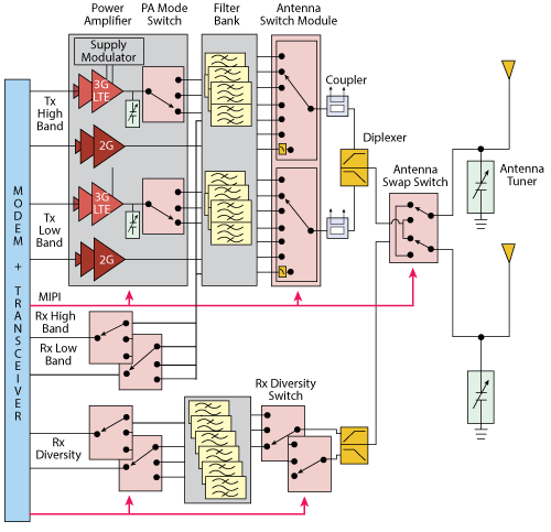
Figure 3 4G/LTE RF FEM architecture.6
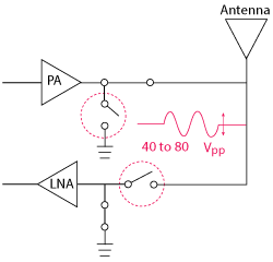
Figure 4 Peak-to-peak voltage with high antenna VSWR.7
Similar provisions for data rate expansion in Wi-Fi networks not only provide a better user experience for data-rich content but also offer a potential means to augment cellular network capacity through offloads to carrier grade Wi-Fi access points. For example, the IEEE 802.11ac Wi-Fi standard has seen significant adoption (projected 13 percent CAGR over 2014-20) since its introduction and, with the Wave 2 specifications, promises data rates up to 3.5 Gbps through the use of multiple-input-multiple-output (MIMO) and channel bonding techniques.4
Can’t We All Just Be Friends?
Enabling the high data rate supported by LTE is driving the complexity we see today in all segments of the RF interface – the front-end module (FEM), in particular, but also the RF transceiver and baseband processor. The complexity in the FEM originates primarily from four sources:
- Increasing number of bands supported per handset (ranging from 2 to 18 LTE bands in addition to legacy 2G/3G bands)
- Introduction of high frequency bands (6 bands at 2.5 GHz and above)
- High peak to average power ratio (PAPR) from OFDM (also used in other UMTS technologies and in Wi-Fi), where the PAPR can be up to 11.5 dB5
- Carrier aggregation (CA) which further enhances the complexity due to the low efficiency of handset antennas of limited size and the demand of long battery life.
The architecture of one of today’s advanced LTE capable smartphones demonstrates this complexity, as shown in the example block diagram of Figure 3. Support for multiple bands in a mobile device requires a complex array of filters and switches with high throw counts to route signals to and from the antenna to the main RF transceiver/baseband for Tx/Rx processing. Within this array of filters and switches, careful consideration must be given to path loss, isolation, stopband rejection and linearity to ensure the fidelity of the signal being processed.
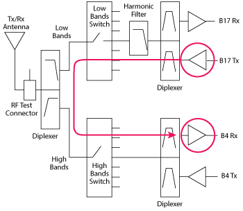
Figure 5 Isolation and interferers challenge the implementation of carrier aggregation with the current LTE band plan.8
The RF switch plays an important role in this architecture by providing high electrical isolation between the “on” channel and other “off” channels, while protecting the highly sensitive receiver channels from the high power transmitter signal. The high peak power of the LTE transmitter (which can reach one watt or more) also generates harmonic frequency components and non-harmonic, intermodulation frequency components, due to the nonlinear behavior of any of the FEM components in the signal path. These include the RF switches and other active and passive components such as tuners, low noise amplifiers (LNA), power amplifiers (PA) and filters. These undesired frequency components drain power from the desired fundamental signal and may also cause saturation in the receiver LNA, depending on power level.
The high peak-to-average ratio of the modulated LTE signal requires that all FEM components have highly linear characteristics. Reduced linearity anywhere in the signal chain requires that the signal be “backed-off” in terms of the average power incident to the device to remain within the linear operating region of the entire signal path. Reduced linearity inherently translates to lower power delivered by the mobile device to the base station on transmit and lower power than can be processed by the receiver baseband processor. Both scenarios can cause dropped calls.
Although not immediately intuitive, signal back-off also affects battery life. Power amplifiers tend to be most efficient when operated at saturated power levels; however, these conditions are worst for linearity. Therefore, for linear transmission, one needs to back off power levels, causing amplifiers to be less efficient. Special techniques such as average power tracking (APT) and envelope tracking (ET) have been employed to adjust the PA bias on a real-time basis according to the envelope of the modulated output waveform, so that the PA always operates near optimum efficiency. These techniques have been implemented with some success. It requires additional computing cycles from the baseband/applications processor to deliver the necessary control to the PA bias controller to accurately track the modulation signal envelope. For improving PA linearity, digital predistortion (DPD) techniques have also been employed in cellular applications. These DPD and ET techniques are emerging in Wi-Fi power amplifier applications as well, significant challenges that need to be addressed.
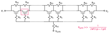
Figure 6 RF SOI device stacking.9
The physical limitation of today’s mobile device form factors have also contributed to the ever changing demands of today’s wireless standards. The Wheeler limit relates the physical dimensions of an antenna structure to its resultant gain and bandwidth. Achieving flat broadband gain and directivity from an antenna, not much larger than a stick of gum, over all 40+ LTE frequency bands is very difficult. In addition, the impedance the antenna presents to the front end components (switch or filter/diplexer) over this frequency range is not constant and can vary greatly, resulting in very high VSWR, up to 20:1. This can result in reflected signals from the antenna appearing at the main antenna RF switch as high as 80 Vpp (see Figure 4). High reverse breakdown is essential in handling these conditions reliably. Techniques such as antenna impedance tuning and aperture tuning have been introduced in some radio architectures to address these issues.
Impedance tuners are typically placed at the antenna port of the main antenna RF switch module and are used to adjust the impedance presented to the PA, measuring the reflected voltage from the antenna by coupling some of the energy into a detector. The impedance is adjusted using fixed tuner settings across the band (open loop) or in real time (closed loop) using active reflected power measurement techniques performed at baseband. Aperture tuners are typically placed at the antenna input port and are used to actively adjust the radiation pattern of the antenna to achieve maximum EIRP in a given direction. Both methods are used to enhance the sensitivity of the mobile device and deliver the best possible signal between the base station and the user.
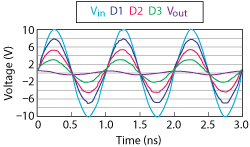
Figure 7 10 V peak-to-peak input across a 4-stack SOI FET, with almost equal voltage drop across the drain nodes of each FET (D1, D2 and D3).7
All the complexities discussed in the cellular FEM (insertion loss, isolation, nonlinearity, antenna bandwidth and mismatch) are compounded by the introduction of carrier aggregation. Carrier aggregation (CA) binds two or more channels simultaneously to enhance the effective bandwidth of the signal and boosting the combined data rate. A similar technique is used in today’s fiber optic networks, where multiple high speed channels are combined to create a single ultra-high speed data stream. Handsets are already being introduced in the market which can support downlink carrier aggregation. In the future, the LTE standard provides for handsets to support uplink carrier aggregation. Handsets supporting either of these requirements must operate efficiently and with good reception characteristics. This can only be achieved by improving these key figures of merit (loss, isolation, linearity) even further.
The complexity associated with CA is evident from a specific example of aggregation between Band 4 and Band 17, a problem raised several years ago, when it was found that the third harmonic of B17 Tx (700 MHz) fell within the B4 Rx (2.1 GHz), prompting tougher constraints on RF switch isolation, out of band interferer rejection and path linearity to mitigate the problem (see Figure 5). Even if the Rx frequency is not a multiple (second, third harmonic, etc.) of the Tx frequency aggregation bands, there can be interference for carrier aggregation frequency pair combinations where the Rx frequency coincides with one of the inter-modulation frequencies of the Tx band. There are a number of carrier aggregation band pairs which fall into this category.
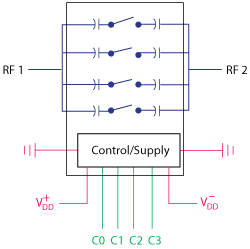
Figure 8 16-state variable capacitor array.7
What About Wi-Fi?
A similar complexity in FEM architectures is seen in 802.11ac Wi-Fi. MIMO channel binding and beamforming techniques are leveraged to maximize signal fidelity, and each of these techniques has its own challenges in implementation. Compared to cellular, Wi-Fi operates at reduced signal power levels (20 dBm maximum user equipment transmitted power compared to 23 dBm for LTE), since coverage is over a shorter distance. However, these systems use complex modulation to support the high data rate (up to 256 QAM in 802.11ac) and a high carrier frequency (5.8 GHz), which require careful system design. The linearity requirement for Wi-Fi 802.11ac power amplifiers is very stringent because of high PAPR and EVM requirements (< 1.8 percent Tx for 256 QAM constellation density). The LNA noise figure and linearity requirements (for RF switches as well) are also stringent due to high levels of interference of overlapping channels, particularly in the 2.5 GHz Band. Together these requirements put significant pressure on overall front-end performance to minimize power consumption and achieve good reception.
In an access point, 802.11ac promises a peak data rate of 6.7 Gbps with 160 MHz bandwidth and an 8 × 8 MIMO configuration, while compatible terminal devices will push 1 Gbps with a 2 × 2 MIMO configuration. These requirements put a significant burden on the PA efficiency and total solution size, which favors silicon integration. In the future, to drive >10 Gbps data rates, the standards being discussed today will either push improved spectral efficiency of 802.11ac transmission (as is being proposed in 802.11ax) or a move to a higher frequency band (802.11ad). For the foreseeable future, the Wi-Fi data rate requirements will place significant pressure on overall front-end efficiency to minimize power consumption and module size.
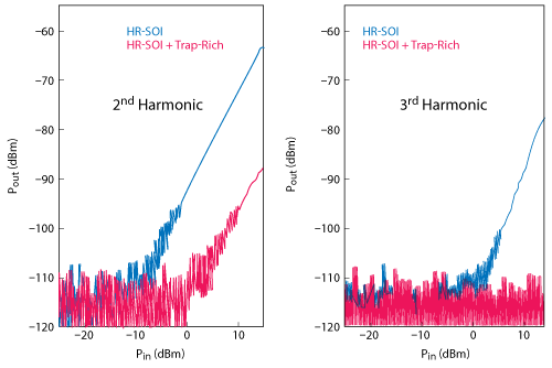
Figure 9 Harmonic distortion of a coplanar transmission line, comparing HR-SOI to HR-SOI with a trap-rich layer.10
Why RF SOI and Why Now?
It is well known that RF SOI has established itself as the technology of choice for cellular and Wi-Fi RF switches in many applications. In the early days of 3G/4G adoption, a new technology was needed that could achieve the same or similar performance in terms of Ft, mobility and breakdown voltage with sufficient manufacturing capacity to meet the expected market demand at a lower cost. Until that point, GaAs PHEMT and PIN diode technologies were used for the RF switch function. The key characteristics that have solidified RF SOI’s role in mobile FEMs are:
- Device stacking ability for higher voltage handling
- Low on-resistance (Ron) for reduced insertion loss
- Low off-capacitance (Coff) and substrate parasitics for high isolation and high Q
- Logic and control integration
- Low cost and improved economics over III-V technologies
- Mainstream silicon manufacturing
It has been covered in the literature9 that RF SOI on a high resistivity substrate with sufficiently high gate resistors allow the FET body terminals to float and allow multiple FET devices to be stacked in order to handle high voltage, high power conditions (see Figure 6).
By combining these inherent properties of RF SOI along with the use of proper bias network design, one can achieve the correct voltage division across the stack in the off state and very low resistance in the on state (Ron) for low insertion loss (see Figure 7). Intrinsic device Ron reduction is achieved fundamentally by lowering channel length, but this must be carefully balanced with the corresponding reduction in BVdss. Reduction in BVdss requires a larger device stack height and chip area in order to maintain the high voltage handling capability. The off state capacitance (Coff) is another key metric in switch design and determines the off state isolation the device can achieve. Reduction in Coff to achieve greater isolation can be challenging and must employ a variety of techniques including junction engineering, device layout and metal stack optimization. Continual reduction in the Ron Coff product while maintaining a reasonable BVdss has allowed complex switch products to be designed.
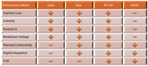
Figure 10 Comparison of key FEM technologies.
With a high quality RF switch that can handle high power levels and achieve low insertion loss with high isolation, one can begin to imagine other applications where this device can be used. By combining RF switches and capacitors in series or in shunt into an array, a selectable or tunable high Q capacitor bank can be created, as shown in Figure 8, that can be used as a dynamic or variable tuning element. Many of today’s RF SOI technologies have high quality metal-insulator-metal (MIM) and metal-oxide-metal (MOM) capacitors with reasonably high density (>2 fF/µm2) and high breakdown voltages to support large standing wave signals. The combination of MIM/MOM capacitors and RF switches makes tuners possible, leading to the adoption of RF SOI for applications such as antenna impedance matching or antenna aperture tuning to address the antenna bandwidth and impedance variability problems.
Both of the applications described require an element of digital control to select a given switch configuration or tuner state. In GaAs or other III-V technologies, this typically requires a separate CMOS controller chip to be paired with the GaAs device to dynamically adjust the device state based on commands from the baseband processor. RF SOI allows the complete monolithic integration of the controller element and the RF function into a single chip, thus reducing cost, space and overall system complexity.
Due to the power levels involved, each of the applications described requires very high linearity and low harmonic response in order to minimize the creation of distortion products in high power, multi-carrier conditions. Today’s LTE system specifications require any harmonics generated by the RF switch to be >70 dB below the main carrier signal. Increased FET breakdown voltage allows reducing stack height and improving insertion loss and related harmonic generation. However, another component of non-linearity is associated with surface charge recombination in the substrate, where high power RF signals can induce the creation of a parasitic conduction layer in the SOI substrate silicon/buried oxide (BOX) interface. RF signals may couple to this parasitic layer and modulate its conduction characteristics. This dynamic has been addressed through various substrate treatments, such as charge trap-injection, which minimize the creation of this parasitic layer at the interface. This has resulted in better than 15 dB improvement in device linearity performance over standard high resistivity substrates without these treatments (see Figure 9).
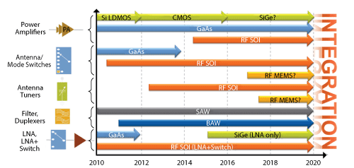
Figure 11 RF FEM technology trends.
RF SOI has enabled the integration of two other critical components of the FEM: LNAs and PAs. The noise figure and gain performance of an LNA is driven by the ft, fmax and gate resistance of the FET. SOI provides a very low capacitance device thereby helping both ft and fmax. Since the early introduction of RF SOI, the Wi-Fi FEM has widely deployed the use of both switches and LNAs integrated on a single IC. With the advent of carrier aggregation in LTE cellular applications, improved LNA performance for both main Tx/Rx and diversity Rx antenna paths is desired. This presents an opportunity for RF SOI to allow the integration of optimized switches and LNAs in the cellular FEM as well. Power amplifiers, on the other hand, need high ft and high breakdown voltages. FET stacking concepts have been demonstrated on high resistivity (HR) substrate RF SOI devices in the literature to provide acceptable cellular PA performance.11 HR SOI also allows improved passives to support on-chip matching. Many challenges related to PA integration on SOI, such as thermal and substrate coupling, have been addressed over time and products have been demonstrated. RF SOI circuit design and architecture innovation are important components of driving these solutions into the mainstream. Of all of the technologies addressing FEM applications today, RF SOI provides a unique balance in meeting key technical and economic requirements (see Figure 10).
The Future for RF SOI
The rapid growth in smartphones and tablet PCs and other mobile consumer applications has created an opportunity and demand for chips based on RF SOI technology, particularly for antenna interface and RF front-end components such as RF switches and antenna tuners. As a low cost and more flexible alternative to GaAs, RF SOI is recognized as the technology of choice for the majority of RF switches and antenna tuners manufactured today for mobile devices.
As wireless standards continue to evolve, there will be tougher challenges ahead across the entire RF SOI value chain including handset providers, RF component makers, SOI foundries and substrate suppliers. The next release of the 3GPP LTE standard (Rel. 13) will pave the way for uplink carrier aggregation. This requirement will push linearity requirements for all FEM components, particularly RF switches, even further than today’s levels (estimates vary between 85 to 90 dBm IIP3).
There will also be specifications defined for LTE operation in the unlicensed bands and require coexistence with Wi-Fi. In parallel, there is a plan in the next phase of Wi-Fi evolution to adopt 1024 QAM modulation which will further raise the bar for linearity and phase noise in Wi-Fi FEM components. All of these standard dynamics will present an interesting challenge for both cellular and Wi-Fi FEM manufacturers in mitigating the coexistence requirements for linearity and receiver sensitivity.
To address these highly complex, multi-band and multi-standard designs, RF front-end modules will require further integration of multiple RF functions like power amplifiers, antenna switches and transceivers, as well as digital processing and power management, to simplify the architecture and lower the cost. Today these functions are addressed by different technologies, but the trends seem to favor a silicon approach to achieve true integration (see Figure 11).
Mobile devices that exploit RF SOI for RF front-end module functions benefit from higher levels of integration that combine with improved linearity and insertion loss and translate to better transmitter efficiency and longer battery life, enabling longer talk times (lower power) and a better user experience. Higher levels of integration also lead to RF circuit and architecture innovation as these technology benefits are combined with digital signal processing to create a dynamically adaptable solution to suit a given set of conditions. These are the clear benefits of a silicon-based technology. The exploration of the capabilities of RF SOI is just beginning.
References
- Cisco White Paper: Cisco Visual Networking Index: Forecast and Methodology, 2014-2019, May 2015.
- Cisco White Paper: Cisco Visual Networking Index: Global Mobile Data Traffic, 2014-2019, February 2015.
- iHS smartphone-electronics-design-intelligence-database, Q2 2015.
- “Cisco Will Ride the 802.11ac Wave,” http://blogs.cisco.com/wireless/cisco-will-ride-the-802-11ac-wave2.
- Sassan Ahmadi, “LTE-Advanced: A Practical Systems Approach to Understanding 3GPP LTE releases 10 and 11 Radio Access Technologies,” Chapter 13, Academic Press, 2014.
- SOITEC White Paper, February 2013.
- Ali Tombak, “Silicon on Insulator (SOI) Switches for Cellular and WLAN Front End Applications,” IMS 2012 Workshop.
- “Recent Advances in RF Front End for D/L Carrier Aggregation,” muRata, IWPC, Lund, Sweden, June, 2013.
- M.B. Shifrin, P.J. Katzin and Y. Ayasli, “Monolithic FET Structures for High Power Control Component Applications,” IEEE Transactions on Microwave Theory and Techniques, Vol. 37, Issue 12.
- J. P. Raskin et al., “RF SOI CMOS Technology on Commercial Trap-Rich High Resistivity SOI Wafer”, 2012 International SOI Conference.
- S. Pornpromlikit et al., “A Watt-Level Stacked-FET Linear Power Amplifier in Silicon-on-Insulator CMOS,” IEEE Transactions on Microwave Theory and Techniques, 2010.