
A DC to 35 GHz mm-wave MMIC Package
Dielectric Laboratories, a Dover Technologies company
Cazenovia, NY
One of the potentially gating issues for implementing MMIC die in high volume commercial and consumer markets is the determination of known good die. It is difficult to reliably RF test the die in wafer form, and testing packaged devices in the typical package is not much easier. A DiPak package has been introduced recently that offers a solution to testing die at functional RF power levels. By incorporating grounded coplanar waveguide into the RF input and output (I/O), assembled devices can be probed using 400 mm pitch probes.
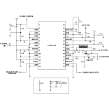 The model M20002 DiPak mm-wave MMIC package has a 0.270" ¥ 0.160" die-mount cavity, six low frequency/DC feedthrus and two mm-wave feedthrus, as shown in Figure 1 . Unlike DiPak models M20001 and M20005, the M20002 package features two grounded coplanar waveguide feedthrus with enhanced high frequency features. These feedthrus provide RF coplanar probe test compatibility for
 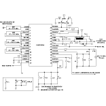 accurate fixtureless testing of assembled modules. Figure 2 shows the return loss and insertion loss of a single I/O RF feedthru with 150 mm pitch launches. The coplanar ground conductors improve RF isolation, reduce feedback and enable higher stable gain within the package.
Figure 3 shows the RF port return loss and port-to-port isolation probed at the exterior ports with internal terminations. The user can enhance performance in the 30 GHz 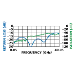 frequency range and beyond by bonding the coplanar grounds at the package I/Os to user circuit board grounds, which reduces ground inductance. The high thermal conductivity copper/molybdenum/copper (Cu/Mo/Cu) base metal and four-hole screw mounting ensure good thermal management (easily handling 10 W) and enable replaceable system construction. The base metal provides a no-compromise, low cost package that is thermal expansion matched (5.7 ppm/°C) to GaAs with high 170 W/m-K thermal conductivity through its thickness and 210 W/m-K thermal spreading.
The DiPak ceramic package features a material system that is optimized for GaAs and silicon multichip modules (MCM) and is particularly well suited to microwave and mm-wave applications. The low dielectric constant/low loss tangent ceramic and low loss thick-film silver conductors enable low loss, low SWR feedthrus. In this unique process, the ceramic is cofired directly to the Cu/Mo/Cu base metal, eliminating x-y shrinkage. Precise x-y features simplify automated assembly, wirebonding and test and enhance mm-wave performance. In contrast, conventional cofired package technologies have x-y shrinkage tolerances that are too large, leading to excessive wirebond lengths and variation and, consequently, poor mm-wave performance.
The DiPak package is based on low temperature cofired ceramic on metal core, which was pioneered by Sarnoff. The technology utilizes a metallic base that constrains the x-y shrinkage. The metallic base is closely matched to the coefficient of thermal expansion characteristics of GaAs, which allows die to be soldered directly to the metallic base for optimal grounding and thermal dissipation.
The M20002 DiPak package is intended for power amplifiers or MCM/MMIC amplifier chains. The product's high performance and low cost make it suitable for use in mm-wave systems such as local multipoint distribution systems, low voltage differential signal digital radios and satellite systems such as Teledesic, Iridium and very small aperture terminals.
Integrated resistors and capacitors already have been demonstrated in the technology and additional packages are expected to be developed shortly with integrated bypass capacitors. While the M20002 package is designed to meet a broad variety of needs, customized cavities are available for a minimal tooling charge.
Dielectric Laboratories, a Dover Technologies company,
Cazenovia, NY
(315) 655-8710.