
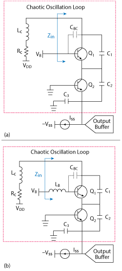
Figure 1 Normal common-base version of the cascode chaotic Colpitts oscillator without base inductor LB (a) and new version with base inductor LB (b).
A wideband cascode chaotic Colpitts oscillator with enhanced negative resistance is demonstrated. The circuit is implemented with InGaP/GaAs HBT technology. The measured fundamental frequency is 2.7 GHz, and the output power spectrum covers the 3.1 to 5.8 and 6.1 to 9 GHz ultra-wideband (UWB) bands. Negative resistance degradation caused by the Miller capacitance is compensated with an optimized base inductor. The fundamental frequency and bandwidth of chaotic oscillation is improved versus a normal common-base oscillator by increasing the voltage swing between the junctions as well as the transconductance of the transistor. This design also reduces power consumption in the oscillation loop.
Chaotic signals are wideband, deterministic, non-periodic and random-like signals derived from nonlinear dynamic systems. They offer a number of attractive features, particularly for UWB applications.1, 2 Several chaotic signal generator design technologies have been proposed to meet bandwidth demands at microwave frequencies. One proposed technology is based on the chaotic Colpitts oscillator.3
Colpitts-based chaotic oscillators have received significant attention in the past decade,4,5,6,7,8 but the performance of a typical chaotic Colpitts oscillator is constrained by the influence of transistor parasitics that limit its fundamental frequency f0.5 To mitigate the influence of parasitics and to increase f0, various design techniques have been proposed including the use of parasitics as parts of the oscillation loop,5 an addition of a series L and diode load to redistribute the effects of base-collector parasitic capacitance CBC,6 and a cascode structure to reduce the Miller effect at CBC.7,8
Improved chaotic Colpitts oscillators have had limited success, however, in increasing f0 and bandwidth, while lowering power consumption. To gain an in-depth understanding of the performance issues and to explore the use of advances in normal oscillator design techniques for chaotic circuits, it is essential to recognize the commonality as well as differences in normal and chaotic oscillator designs.
A non-chaotic Colpitts oscillator exhibits a sharp decrease in negative resistance at high frequencies due to the Miller effect at CBC, limiting its maximum oscillation frequency.9 The effect appears in chaotic Colpitts oscillators as well. Unlike a normal narrowband oscillator, however, a serial resistor is often included in the oscillation loop of a chaotic Colpitts to satisfy the requirement for broadband chaotic oscillation. This leads to a low Q and high power losses in the loop. The broadband oscillation requirement in a chaotic circuit imposes the need for a higher negative resistance than in a normal oscillator. Thus, the challenge in a chaotic circuit design is to determine a proper and sufficient negative resistance for overcoming resonator losses in order to reach a start-up chaotic oscillation and optimize f0.
A cascode chaotic Colpitts oscillator design is introduced with two separated inductors connected at the base and collector nodes respectively. Tuning of these two inductors enhances negative resistance to compensate for its degradation from the decrease of transistor transconductance (gm) at high frequencies and maximizes the fundamental frequency f0. The enhancement of gm with base inductance reduces the need for a higher bias voltage and current, thus lowering resonator power consumption. Measurement results demonstrate operation from 1.3 to 9 GHz, covering the 3.1 to 5.8 and 6.1 to 9 GHz UWB bands.
CIRCUIT DESIGN
Figure 1a represents a normal chaotic Colpitts oscillator design,7,8 while Figure 1b shows the new cascode chaotic Colpitts oscillator design. The chaotic circuit of Figure 1b evolves from a traditional normal common-base cascode Colpitts oscillator by including an additional inductor LB at the base node. The bias current ISS is controlled by tuning the voltage source VSS. In contrast to a standard common-base chaotic Colpitts design,4,6,7,8 this circuit has two important design features. First, the parallel equivalent inductance of LC-RC and LB-CBC is smaller than that of LC and LB. Without significantly impacting the fundamental frequency f0, the gm of the transistor can be enhanced by increasing LB. Consequently, the negative resistance is enhanced by increasing the voltage swing between the junctions as well as the gm of the transistor. Second, the enhancement of gm with LB reduces the demand for higher VDD and ISS, thus lowering power consumption of the oscillation loop.
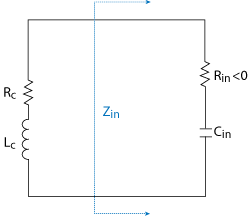
Figure 2 Equivalent circuit of the chaotic oscillation loop.
NEGATIVE RESISTANCE ANALYSIS
Figure 2 shows the equivalent circuit of the chaotic oscillation loop in Figure 1b. The input impedance Zin between base and collector nodes can be viewed as an equivalent circuit of a negative resistance Rin in series with a capacitance Cin.
Rin of the normal common-based circuit in Figure 1a can be expressed as:
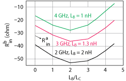
Figure 3 Calculated negative resistance vs. LB/LC.
Rin of the circuit in Figure 1b can be expressed as:
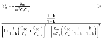
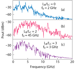
Figure 4 Simulated output power spectrum vs. LB/LC.
where CBE and CBC are base-emitter and base-collector parasitic capacitance respectively, f is the oscillation frequency of the loop; Q1 and Q2 are the same transistors.
When LB = 0 nH,
Equation 5 shows that the equivalent circuits of the two chaotic oscillators in Figure 1 are the same without considering LB. From Equations 2, 3 and 4, we can calculate the negative resistance Rin (2 µm InGaP/GaAs HBTs with fT=29.5 GHz, CBE=0.49 pF and CBC=0.28 pF are used in calculation). Figure 3 shows the negative resistance Rb in dependenceon the ratio of LB/LC. Each curve is generated by fixing the value of LC and the oscillation frequency. Ra in is a constant value with fixed oscillation frequency. When the LB/LC ratio equals zero, Rb in and Ra in are the same as shown in Equation 5. The equivalent circuit of LB-CBC is capacitive and its impedance is inversely proportional to LB. When LB is small, -Rb in increases with LB because the impedance of LB-CBC is much larger than -Rb in and its decrease in value can be neglected. Thus, -Rin is mainly dominated by the transistor gm, which is directly proportional to LB and the voltage, current swing in the circuit. However, when LB is large, -Rb in decreases as LB increases, because the impedance of LB-CBC is too low to be neglected and the voltage and current swing and gm enhancements become saturated. -Rb in is mainly determined by the impedance of LB-CBC, decreasing with increasing LB. An optimum LB/LC ratio is observed for the maximum negative resistance. When LB is 2 to 3 times LC, -Rb in is improved by almost 50 percent over -Ra in. Therefore, with an optimum LB/LC ratio, LC, C1, C2 and C3 are reduced to increase the chaotic oscillation frequency.
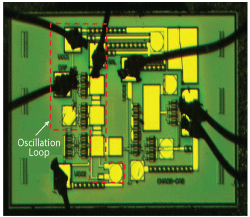
Figure 5 Photograph of the fabricated 0.6 × 0.6 mm circuit.
Figure 4 shows the simulated output power spectrum of the circuit. Transistors used in this simulation are the same as aforementioned InGaP/GaAs HBTs. When LB/LC=0, the highest fundamental frequency f0 for chaotic oscillation is only 2 GHz. When LB/LC=2, f0 increases to 4.5 GHz. When LB/LC = 3, f0 decreases to 3 GHz. From these simulation results, an optimum LB/LC ratio is observed for the maximum fundamental frequency f0, which is consistent with calculated results in Figure 3.
MEASUREMENT RESULTS
The proposed cascode (with LB) and the normal common-base (without LB) chaotic Colpitts circuits are implemented with 2 µm InGaP/GaAs HBT technology. Figure 5 is a photograph of the fabricated 0.6 × 0.6 mm chip. As chaotic circuits are extremely sensitive to circuit elements, LB, LC and RC in Figure 1 are not designed into this chip, enabling adjustment of LB, LC and RC values on the PCB to fit chaotic oscillation start-up conditions.
To optimize the fundamental frequency, f0, the values of the loop inductances LC, LB, capacitances C1, C2, C3 and the loss resistance RC are chosen based on the concept previously outlined. Note that the effect of parasitic base-emitter capacitance CBE has been considered in choosing capacitance. VDD is fixed and VSS is adjusted to achieve the desired output chaotic signals. Figures 6a and 6b show the measured output power spectrum of the normal cascode circuit without LB and the proposed circuit with optimized LB, respectively. In Figure 6a, LB = 0 nH, LC = 5 nH, RC = 25 Ω, C1 = 3 pF, C2 = 3 pF, C3 = 3 pF, VDD = 10 V, ISS = 16 mA and f0 = 1.6 GHz. In Figure 6b, LB = 2.7 nH, LC = 1.3 nH, RC = 22 Ω, C1 = 2 pF, C2 = 2 pF, C3 = 2 pF, VDD = 7 V, ISS = 12 mA and f0 = 2.7 GHz.
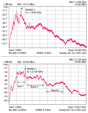
Figure 6 Measured output power spectrum of the normal cascode circuit without LB (a) and with the optimized LB (b).
The optimum LB of 2.1 times LC is consistent with calculated results in Figure 3 and simulation results in Figure 4. The fundamental frequency f0 is 1.6 GHz and 2.7 GHz for circuits without LB and with optimum LB, respectively, illustrating an increase in f0 of 69 percent. Using the chaotic bandwidth (BW) definitions in Mykolaitis et al.,4 and Bumeliene. et al.,8 frequency bands of the output power spectra are: Band 1: 1.3 to 2.7 GHz, Band 2: 2.9 to 5.8 GHz and Band 3: 6.1 to 9 GHz as shown in Figure 6b. Band 2 and Band 3 cover the 3.1 to 5.8 GHz and 6.1 to 9 GHz UWB bands respectively. Wire inductance and parasitic resistance on the circuit board may be causes for a lower measured f0 than simulated.
Figure 7 shows the double scroll attractor of the proposed circuit measured with an oscilloscope. Circuit elements are the same as in Figure 6b. The horizontal axis (200 mV/div) represents the collector voltage of Q1 and the vertical axis (100 mV/div) is the base voltage of Q1. The double scroll attractor confirms that the oscillation is chaotic.
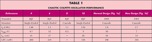
Table 1 compares the performance of this design with recently published microwave chaotic Colpitts oscillators.4,6,8,10 The fundamental frequency f0 for this design is much higher. Excluding power consumption of the current source and output buffer, the loop power consumption (LPC) is estimated by (VDD+0.8 V) × ISS in a Colpitts circuit using BJTs and by (VDD+1.6) × ISS in a Colpitts circuit using HBTs. LPC in this design is much lower compared to the others represented in the table.4,6,10 This power reduction is attributed to an increased gm with an optimum base inductor alleviating a sharp decrease at reduced bias voltage VDD and current ISS.
CONCLUSION
A cascode Colpitts oscillator with enhanced negative resistance is designed for the chaotic oscillator. Theoretical calculation shows that the negative resistance degradation at high frequencies is compensated by increasing the voltage and current swing in the circuit and the transconductance of the transistor via an optimum base inductor. With enhanced negative resistance, the fundamental frequency f0 is increased to 2.7 GHz. The circuit operates from 1.3 to 9 GHz, covering the 3.1 to 5.8 and 6.1 to 9 GHz UWB frequency bands. This design also reduces power consumption in the oscillation loop.
ACKNOWLEDGMENTS
This work was supported by the National Science Foundation of China under Grant No. 11074122.
REFERENCES
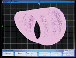
Figure 7 Measured double scroll attractor (horizontal axis = 200 mV/div, vertical axis = 100 mV/div).
- C. C. Chong, S. K. Yong and S. S. Lee, “UWB Direct Chaotic Communication Technology,” IEEE Antennas and Wireless Propagation Letters, Vol. 4, 2005, pp. 316–319.
- C. C. Chong and S. K. Yong, “UWB Direct Chaotic Communication Technology for Low-Rate WPAN Applications,” IEEE Transactions on Vehicular Technology, Vol. 57, No. 3, May 2008, pp. 1527–1536.
- A. S. Dmitriev, B. Y. Kyarginsky, A. I. Panas and S. O. Starkov, “Experiments on Direct Chaotic Communications in Microwave Band,” International Journal of Bifurcation and Chaos, Vol. 13, No. 6, 2003, pp. 1495–1507.
- G. Mykolaitis, A. Tamasševičius and S. Bumeliene., “Experimental Demonstration of Chaos from Colpitts Oscillator in VHF and UHF Ranges,” Electronics Letters, Vol. 40, No. 2, January 2004, pp. 91–92.
- A. Tamasševičius, S. Bumeliene. and E. Lindberg, “Improved Chaotic Colpitts Oscillator for Ultrahigh Frequencies,” Electronics Letters, Vol. 40, No. 25, December 2004, pp. 1569–1570.
- E. Lindberg, A. Tamasševičius, G. Mykolaitis and S. Bumeliene., “Towards Threshold Frequency in Chaotic Colpitts Oscillator,” International Journal of Bifurcation and Chaos, Vol. 17, No. 10, 2007, pp. 3449–3453.
- A. Tamasševičius, G. Mykolaitis, S. Bumeliene., A. Čenys, A. N. Anagnostopoulos and E. Lindberg, “Two-stage Chaotic Colpitts Oscillator,” Electronics Letters, Vol. 37, No. 9, April 2001, pp. 549–551.
- S. Bumeliene., A. Tamasševičius, G. Mykolaitis, A. Baziliauskas and E. Lindberg, “Numerical Investigation and Experimental Demonstration of Chaos from Two-stage Colpitts Oscillator in the Ultrahigh Frequency Range,” Nonlinear Dynamics, Vol. 44, 2006, pp. 167–172.
- Y. Chen, K. Mouthaan and B.L. Ooi, “A Novel Technique to Enhance the Negative Resistance for Colpitts Oscillators by Parasitic Cancellation,” IEEE Electron Devices and Solid-State Circuits Conference, December 2007, pp. 425–428.
- W.L. Chen, Y. Guo, H. Gao and G.P. Li, “A Novel Ultra-Wideband Microwave Chaotic Colpitts Oscillator,” IEEE Wireless and Microwave Technology Conference, April 2013.