
Coupling Behavior between Transmission Lines with Meshed Ground Planes in LTCC-MCMs
Multilayer ceramic modules for high speed digital applications use meshed planes between the signal layers for shielding and power supply. Both wave impedances of the signal lines and coupling behavior between different signal layers are influenced by the properties of these meshed planes. Former investigations have shown that for a constant metallization rate (aperture ratio) and a given line width, the wave impedance is nearly constant over a wide range of grid pitches. The coupling behavior (near- and far-signal crosstalk) is explained by practical investigations of different test modules and three-dimensional (3-D) time-domain field simulations. It has been observed that coupling between layers depends on the metallization rate and the position of lines over the grid. One aim is to determine the optimal configuration for minimum couplings.
H. Thust, K.H. Drüe, J. Müller, T. Thelemann and T. Tuschick
Technical University of Ilmenau, Germany
J. Chilo, C. Golovanov and F. Ndagijimana
ENSERG Grenoble, France
Due to the increasing speed of signals for a variety of applications in the telecommunications and computer fields, more attention must be paid to coupling mechanisms inside interconnection structures. Closely related to this topic is the impedance control of lines to avoid strong reflections within single lines. Ceramic-based multilayer circuits composed of high temperature cofired ceramics (HTCC) or low temperature cofired ceramics (LTCC) (also known as a multichip module with cofired substrate (MCM-C)) combine the good electrical properties of ceramics at high frequencies with precise control of the dielectric's thickness. According to the lower process temperature (< 900°C), LTCC has the added advantage of making use of low resistive conductor systems (Ag, Au). In addition, LTCC contains a large amount of glass, which lowers the relative permittivity of the material. Thus, the velocity of the propagated signals is increased compared to HTCC circuits.
The design of such a multilayer circuit requires the designer to consider a set of electrical and technological constraints. One essential modification of ideal conditions is necessary for ground/power planes: They are realized as meshed structures. The ground plane pattern influences both the wave impedance of the transmission lines and the coupling between lines. Coupling is now possible for parallel lines within one layer (edge coupling) and between different signal layers through the ground plane (side coupling).
This article focuses on the investigation of the coupling between different signal layers. Due to the influence of the ground mesh, this type of coupling cannot be described with a closed-form equation. The evaluation of the coupling effect is made possible only by practical tests with useful designs or by sophisticated electrical field simulations. Both methods are applied in this article.
MCM-C Configurations
The reasons to avoid complete ground plane areas are attributed mainly to the ceramic technology. According to tape manufacturers, the metallized area should be below 50 percent. On one hand, this constraint is necessary to maintain enough tape-to-tape contact during lamination to achieve a good bond between adjacent layers. On the other hand, this limit is required to control the shrinkage of the substrate. LTCC tapes shrink laterally during firing by approximately 12 to 15 percent. Due to the different shrinkage and expansion behavior of glass and metal during firing and cooling, an excessively high content of silver paste could force the substrate to shrink even more. This scenario leads either to a deformation of the circuit carrier or to positioning problems in the mounting process of ICs and other additional components.
However, from an electrical point of view, a need exists for numerous vias passing through the ground and power planes to connect the signal layers amongst each other. Applications in HTCC with up to 70 layers and approximately one million vias are known.1 Each via requires a particular opening in the ground plane to avoid shorts. As long as meshed ground planes are used, this via opening requirement is not a problem. The mesh openings serve as placement areas for vias.
A typical signal layer and ground plane structure is shown in Figure 1 . The line 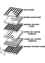 type on the top of the substrate is microstrip. The second layer (embedded microstrip) establishes the signal distribution perpendicular to the first layer (x direction). This hierarchy of alternating signal layer orientation is continued over all layers. Transmission lines that are unsymmetrically embedded between ground planes are known as off-center striplines.
The impedance of the lines is controlled by the ratio of line width w to dielectric thickness h.  Compared to the ideal case with full ground planes, the line inductance is increased and the line capacitance is decreased. This effect can be accounted for by introducing an increased effective thickness heff.2 Prior investigations also revealed that the impedance of the transmission lines is very sensitive to their position relative to the ground plane pattern. All of the following considerations are restricted to the arrangement shown in Figure 2 (aligned with mesh segments) where the aperture ratio ar of the ground plane mesh is expressed as
ar = (pm - wm )2 /(pm 2 )
Coupling of lines can be observed for parallel lines within one layer and between lines in adjacent layers with a common signal distribution (x, y direction). The first coupling form can be described accurately by a set of known closed-form equations using the effective dielectric thickness (edge coupling). Coupling through the ground plane is possible due to openings in the mesh, but a mathematical description of this effect is not available. The lack of prediction of the interaction between signal layers reduces the credibility of signal integrity tests.
The practical and theoretical investigations of this effect have been limited to  three different layouts with a constant ground mesh aperture ratio ar equal to 64 percent and constant line widths. Figure 3 shows the five-layer structure with its dimensions.
The connections to the test fixture for measurement were provided by small sections of microstrip on the top layer connected through vias. All layers have a permittivity of approximately 7.8. The material applied was DuPont 951 with the silver ink system (vias and conductors). The investigation was limited to the coupling between the buried microstrips and the lower off-center stripline (between lines a and b, c or d, respectively). This case is very close to stripline-to-stripline coupling, but has the advantage of a low number of layers necessary for practical tests. Table 1 lists the line- and mesh-related data.
|
Table I | |||
|
Substrate No. |
1 |
2 |
3 |
|
Mesh width wm (m m) |
90 |
180 |
270 |
|
Mesh pitch pm (m m) |
450 |
900 |
1350 |
|
Distance line b to c (m m) |
450 |
900 |
1350 |
|
Distance line c to d (m m) |
900 |
1800 |
2700 |
|
Coupling length (mm) |
40 |
40 |
40 |
Electromagnetic Field Simulation
In order to avoid the manpower of manufacturing the test substrates needed to determine the optimized configuration of a multilayer circuit with meshed ground planes, a numerical tool set was used. The software, based on a transmission line matrix (TLM) of electromagnetic field modeling, allows a design to meet all functional objectives and external constraints simultaneously.
The simulator is a general-purpose 3-D TLM program for time-domain analysis of arbitrarily shaped 3-D electromagnetic structures. It computes the time response of such structures to arbitrary excitation in space and time and extracts their frequency characteristics (such as S parameters and return loss) via discrete or fast Fourier transforms.3 The simulator also visualizes the time evolution of the field distribution in a generated-solution mode for field animation in time.
Measurement vs. Simulation
The accuracy of comparing measurement and simulation results is influenced mainly by measurement errors that include reflections on the test fixture transitions (SMA to microstrip adapter), deviation of lines from the desired 50 W impedance (due to printing technology), reflections inside the structure at discontinuities (via connections from inner to outer layers) and self-resonance effects inside the test structure caused by ground mesh interconnections. Differences in geometrical dimensions between reality and simulation are an additional source of error. One major drawback is attributed to the computation power. It is not possible to simulate the entire structure with all transitions and ground plane interconnections. Only a small section of the coupled lines is taken into consideration. The expected behavior for the full coupling length is obtained mathematically.
The geometrical characteristics of the simulated layout were shown previously. The coupling behavior for the three structures whose mesh dimensions and line distances were listed previously was evaluated. The permittivity of the real substrate was considered (er = 7.8), the lines were matched (in the finite TLM domain, the reflection coefficient is theoretically G = 0) and the exciting signal in line a was a square sinus considering the rise time of the time-delay reflectometer (TDR) oscilloscope signal. A direct comparison was then made between the  TDR measurement (using conventional matched impedances) and simulation results. The results of this comparison are shown in Figure 4 . The backward- and forward-coupled signal in line c was selected to be displayed using the first geometry described in the table. Despite the perturbations caused by the circuit's environment (connectors and discontinuities), good agreement was achieved before calculating the S parameters.
Visualizing the chart of the electromagnetic field, it is obvious that the width of the lines of the meshed ground plane (being equal to the width of the microstrip line) cannot assure a good confinement of the electromagnetic field under the microstrip. Therefore, the lines of the electromagnetic field pass through the ground plane mesh, favoring the coupling phenomena. It is also recognized that the radiation phenomena in the discontinuities (all the intersection lines in the meshed ground plane) are increased with the number of strip junctions.
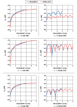 The crosstalk phenomena were characterized by S31 and S41 scattering parameters calculated from reflected and transmitted signals in the appropriate reference planes.4 Figure 5 shows a comparison of near- and far-end measurements and simulations for a grid pitch of 900 mm. The measured values are in good agreement with simulated data. The measurements were performed only in a frequency range up to 3 GHz due to resonance effects. As expected, the magnitude of the coupling signal is
  strongly dependent on the dimensions of the ground plane mesh for a constant rate of metallization (the signal being stronger with increasing mesh pitch pm ).
Figure 6 shows the coupling behavior between lines a and c for different grid pitch values. As expected, the shielding effect of a grid with wider structures is better, but the use of grids with large grid widths is limited by the desired wiring density and resonance effects at higher frequencies.
 Figure 7 shows a possible configuration produced by choosing an adapted geometry that has both dense wiring and good isolation between lines. The coupling behavior of two equidistant line pairs is compared. The coupling between lines c and d using a ground grid pitch of 450 mm and the coupling between lines b and c using a ground grid pitch of 900 mm are displayed. In this case, the use of the smaller grid pitch is advantageous.
Conclusion
The influence of the properties of a meshed plane on the coupling behavior between different signal layers in a multilayer device has been investigated. Practical and numerical investigations were made in both time and frequency domains - first, to establish the influence of the dimensions of the ground plane mesh for a constant rate of metallization and, secondly, to assure that expensive manufacturing of a device and the lack of accuracy of the practical measurements are avoided by using numerical simulations. The usefulness and accuracy of the numerical analysis in the characterization of multilayer interconnecting lines with a meshed ground are proved through the direct comparison between measurements and simulation results.
The first recommendation generated from these results is to realize a necessary increase in the constant rate of metallization produces an increase in the width of the mesh cells. In this case, the lines of the electromagnetic field are better confined under the microstrip line (due to the increased ratio of the width of the ground plane and the width of the microstrip line). However, due to fabrication and process constraints, the aperture ratio is limited to 64 percent. Further simulations will determine an optimum ground mesh geometry within practical technology boundaries. The coupling coefficient of adjacent transmission lines is equal despite the coupling type (edge/side coupling2). This fact simplifies the design and verification of high speed layouts.
References
1. B. Mussler and D. Schwanke, "Recent Development of Nonactive Integrated Components in Multilayer Modules," Proceedings of the International Symposium on Tantalum and Niobium, Goslar, September 24-28, 1995.
2. J. Müller et al., "Line Impedance Control in MCM-Cs with Meshed Ground/Power Planes," Proceedings of the International Conference on Multichip Modules, Denver, CO, April 1996.
3. F. Ndagijimana and P. Saguet, "The Use of a Full-wave 3-D Technique in a CAD-oriented Analysis: The TLM Method," Software Applications in Electrical Engineering, Computational Mechanics Publications, Southampton, 1993.
4. C. Boussetta, F. Ndagijimana, J. Chilo and P. Saguet, "Electrical Modeling Packaging Discontinuities: A General Methodology Based on the Three-dimensional TLM Concept," International Journal of Microwave and Millimeter-wave Computer-aided Engineering, John Wiley & Sons Inc., Vol. 5, No. 2, 1995, pp. 93-103.