
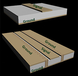
Figure 1 Microstrip (top) and GCPW (bottom) transmission-line circuits.
This article examines how different circuit material characteristics, configurations and fabrication influences can affect the performance of a printed circuit board at millimeter wave frequencies.
Millimeter wave (mmWave) frequencies are being used more and more, for short-range links and high data-rate near field communications (NFC) applications. Suppliers of mmWave integrated circuits (IC) are supporting this growth with more cost-effective components and improved performance. For circuit designers working with these higher frequency ICs, it is important to understand the limits and capabilities of the printed circuit boards (PCBs) and circuit materials that will be used at mmWave frequencies. Numerous PCB issues – insertion loss, dispersion, suppression of spurious wave propagating modes, signal launch effectiveness, fabrication methods – can affect the performance of a circuit at mmWave frequencies. This report will briefly review some of key PCB parameters and what to consider in a PCB material slated for use at mmWave frequencies.
Microstrip vs. GCPW
mmWave circuits can be quite complex, performing transmit and receive functions with advanced modulation, and with frequencies through 77 GHz being used more routinely for short-range applications. However, all of these high frequency circuits share the need for transmission-lines to connect mmWave ICs to power supplies, antennas, input and output ports and other circuits. In general, microstrip and stripline transmission-line technologies are used in microwave circuits through about 30 GHz, while grounded coplanar-waveguide (GCPW) transmission-line technology is used for circuits above 30 GHz. Figure 1 compares microstrip and GCPW transmission-line approaches for a single circuit dielectric layer with metalized ground and circuit conductors. In actual applications, a PCB is more likely to be multilayer, with microstrip or GCPW circuitry on the outer layers of the multilayer construction.
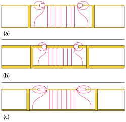
Figure 2 GCPW E field intensity with a small space (tightly coupled) between the adjacent ground and signal with thin copper (a) tightly coupled with thick copper (b) and loosely coupled with thin copper, which will have the least E field coupling (c).
In general, microstrip circuits are susceptible to radiation at mmWave frequencies, where a well designed GCPW circuit is less likely to radiate or suffer radiation loss. Yet, microstrip transmission-line circuits are less likely to have performance affected by PCB fabrication tolerances at mmWave frequencies than GCPW circuits. Fabrication tolerance issues can also be a function of frequency. Transmission lines used for 60 GHz communications backhaul can be affected less by fabrication tolerances than transmission-lines for automotive radar at 77 GHz (with their finer dimensions at higher frequencies).
Effective Dielectric Constant
The comparison is not so much related to the frequency difference of these applications but to a critical circuit property that will change from circuit-to-circuit due to PCB fabrication effects. One circuit property that is prone to change more for a GCPW circuit than for microstrip, due to PCB fabrication effects, is the effective dielectric constant. This is the dielectric constant exhibited by an electromagnetic (EM) wave on the transmission-line due to the EM fields propagating through a combination of the dielectric substrate material (with a dielectric constant of greater than 1) and the air around it (with a dielectric constant of 1). Variations in the effective dielectric constant will affect signal phase through the circuit, causing phase variations. For the transmission-line used for 60 GHz backhaul, variations in phase are important but not as critical as for 77 GHz automotive radar. This may be one reason why 77 GHz automotive radar applications typically use microstrip structures.
One PCB fabrication parameter that causes circuit-to-circuit variation of effective dielectric constant and changes in the phase response is from the variation of copper plating thickness. When a PCB employs plated-through holes (PTH), e.g., for ground connections, the holes are drilled from top to bottom through the PCB. The holes are plated with conductive copper, resulting in lot-to-lot and even circuit-to-circuit copper plating thickness variations. The thickness variations have minimal impact on the effective dielectric constant of microstrip transmission lines. However, since GCPW transmission-line circuits have coupled features, plating thickness variation can cause significant variation in the coupled energy.1 When considering the electric fields between the coplanar layer of a GCPW circuit, the amount of electric field energy between adjacent ground and signal conductors on the coplanar layer will be less with thinner copper and exhibit greater field intensity with thicker copper. Essentially, coupled conductor sidewalls are taller for thicker copper and shorter for thinner copper. Additionally, a small (tightly coupled) space between the adjacent ground conductor and the signal conductor will result in higher electric field intensity in the coupled area, with less coupled energy in loosely coupled areas (i.e., with wide spacing between conductors), as depicted in Figure 2.
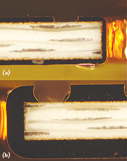
Figure 3 Tightly coupled GCPW circuits with purposely thin (a) and thick (b) copper plating, using 10-mil thick Rogers RO4835 laminate.
A simple study was performed using 10 mil thick (25.4 mm) Rogers RO4835TM laminate with microstrip and GCPW transmission-line circuits purposely fabricated with varying copper plating thickness. The GCPW circuits were tightly and loosely coupled, with thin and thick copper. The circuits were made on the same sheet of circuit material, cut in half with one half of the sheet containing thin plated circuits and the other half containing thick copper circuits. Evaluating circuits made from the same sheet of laminate helps minimize circuit material variables. The total copper thickness of the circuits, which included the base copper thickness of the laminate and the plated copper thickness from the fabricator, was 1 mil for thin copper circuits and 4.1 mils for thick copper circuits.
Figures 3a and b show a cross-sectional view of tightly coupled circuits with thin and thick copper plating respectively. The sidewalls of the adjacent coplanar ground-signal conductors will have more electric field intensity for a circuit with the thicker copper. The impact of air on the effective dielectric constant will be more significant on the circuit with thick copper plating, resulting in a lower effective dielectric constant, than on the circuit with thin copper plating. For loosely coupled circuits, the circuit experiencing the least impact on effective dielectric constant due to air will be the loosely coupled circuit with thin copper.
Wideband measurements were made on these fabricated circuits from 10 MHz to 110 GHz using a Keysight N5251A mmWave vector network analyzer (VNA). The effective dielectric constant was calculated using the differential phase length method.2 The trends for the different circuits remain stable but did vary where return loss was better or worse. Figure 4 shows the performance of the four circuit groups in the range of mmWave frequencies where all circuits had good return loss. The legend for Figure 4 denotes the nominal conductor width (w) and the adjacent coplanar space (s) of the design. For example, the tightly coupled GCPW with thick copper is noted as “w18s6 thick cu.” It has a conductor width of 18 mils and spacing of 6 mils. Of the four circuit groups, the w18s6 circuit should have the greatest electric field intensity in the coupled area, since it is tightly coupled and uses thick copper. This was verified for the circuits with the lowest effective dielectric constant. Since air has a dielectric constant of approximately 1, the more air used for electric field propagation in the GCPW circuit coupling, the lower the effective dielectric constant will be. In contrast, for the loosely coupled circuits with thin copper, the “w21s12 thin cu” circuit should have the lowest electric field intensity and the highest effective dielectric constant.
The microstrip circuits included in this study were not plotted in Figure 4, but those circuits showed a difference in effective dielectric constant of about 0.011 at 67 GHz for circuits with thin and thick copper. In comparison, for the tightly coupled GCPW circuits with thin and thick copper, the difference in effective dielectric constant was approximately 0.100. The loosely coupled GCPW circuits with thin and thick copper had a difference in effective dielectric constant of 0.075. Figure 4 shows that copper plating thickness variations that are part of PCB fabrication are more significant for tightly coupled circuits than for loosely coupled circuits and much less significant for microstrip transmission line circuits than for GCPW circuits.
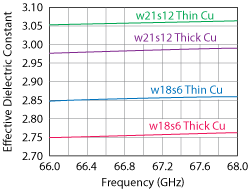
Figure 4 Effective dielectric constant vs. frequency for four groups of GCPW with tight coupling (s6), loose coupling (s12) and thin and thick copper.
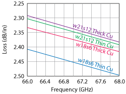
Figure 5 GCPW circuit insertion loss vs. coupling and copper thickness.
The effects of copper plating thickness variation on effective dielectric constant will also apply to the phase response of a circuit. The resulting phase variations can be tolerated for some circuits, but not for others.
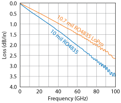
Figure 6 Insertion loss vs. copper surface roughness, comparing Rogers RO4835 laminate and a similar laminate with smoother copper (LoPro).
Insertion Loss
Insertion loss is another concern in addition to phase and effective dielectric constant variation due to copper plating thickness. As air is the lowest loss propagation medium, a circuit that uses air more effectively for propagation will suffer less loss than a circuit which propagates energy through circuit materials. Figure 5 compares the insertion losses of the four GCPW circuits. The circuit with the highest loss is the “w18s6 thin cu” circuit, which has the narrowest conductor (18 mils wide) and the least propagation through air, due to its thin copper plating. The circuit with the least amount of loss is the “w21s12 thick cu” circuit, with a wider conductor, achieving lower conductor loss, and thick copper, which has greater propagation through air.
Copper surface roughness impacts insertion loss and phase propagation.3 The copper surface of interest is the copper-substrate interface between the laminate copper and substrate. A smoother copper surface exhibits less conductor loss, resulting in lower circuit insertion loss for that material. Many mmWave applications are sensitive to insertion loss, and the previous information using 10 mil thick RO4835 circuit material is based on a circuit laminate with a relatively rough copper surface (although it is also available with smoother copper). The copper surface roughness for standard 10 mil thick RO4835 laminate is approximately 2.8 µm root mean square (RMS), and that RMS roughness measurement is the same as the parameter that copper suppliers refer to as Rq. The 10.7 mil thick RO4835LoPro® laminate uses the same substrate as standard RO4835 laminate, although with a much smoother copper surface of approximately 0.8 µm RMS. Figure 6 shows differences in insertion loss from copper surface roughness. The circuits using RO4835 LoPro with smoother copper have lower insertion loss than those with rougher copper. The ripple in the insertion loss response is partly due to imperfect signal launch and spurious wave mode interference.
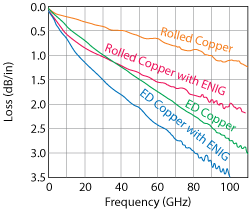
Figure 7 Insertion loss vs. roughness using 5 mil thick RO3003 laminate and showing the impact of ENIG.
Suppression of spurious wave mode propagation is one reason why circuit designers use thinner substrates at higher frequencies. Thinner laminates are also beneficial for minimizing radiation losses, although the tradeoff is an overall increase in insertion loss. Thinner laminates tend to be dominated by conductor losses, so decreasing the copper surface roughness on a thin circuit laminate can provide much greater benefits in lowering insertion loss than decreasing copper surface roughness on a thicker laminate. A high frequency circuit material commonly used at 77 GHz is 5 mil thick Rogers RO3003TM laminate. The thin circuit material suffers less radiation loss than thicker materials, with better spurious mode suppression and easier signal launch optimization. However, it is more sensitive to conductor effects, such as copper surface roughness and plated finish losses.
The previous discussion is based on circuits with bare copper, but real world circuits usually incorporate a plated finish. When a plated finish is added to copper, it typically increases the copper conductor loss and ultimately the insertion loss. The increased conductor loss depends on substrate thickness: thinner circuits are dominated by conductor effects.
Figure 7 shows a combination of information for thin circuits at millimeter wave frequencies. The differences in copper surface roughness are 1.8 µm RMS for the circuits with electrodeposited (ED) copper and 0.3 µm RMS for the rolled copper. The differences in insertion loss are apparent for the two different copper types. The use of a finish will also affect insertion loss. With an electroless nickel/immersion gold (ENIG) finish, nickel has one-third the conductivity of copper, which increases conductor loss. Since the circuit is relatively thin, the increased loss due to ENIG is more significant than if the circuit were thicker. An ENIG finish increases conductor loss for microstrip because of the high current density at the edges of the conductor. With a GCPW circuit, the coupled fields actually use four layers of ENIG finish; because of these added layers, the insertion loss is more dramatically increased than for a microstrip circuit. Figure 8 shows a comparison of microstrip and GCPW and the differences between bare copper and ENIG. GCPW suffers a much greater increase in insertion loss due to an ENIG finish than microstrip. The loss plots in Figure 8 represent 50 ohm transmission-line circuits; the GCPW circuits are tightly coupled. For a GCPW transmission line that was loosely coupled, the impact of ENIG is reduced, with less current density in the coupled area.
Conclusion
At mmWave frequencies, some standard circuit fabrication variables can affect the performance of certain circuit configurations more or less than others. For example, copper thickness variations can affect the performance of GCPW transmission-line circuits. Designers working with small coupled areas, such as GCPW launch or gap coupling, will also be influenced by this variable. Also, circuit substrate thickness can impact wideband insertion loss, as well as the copper surface roughness and the plated conductor finish used on a PCB. For optimum mmWave circuit performance, understanding these variables and how they affect circuit performance will benefit mmWave circuit designers.
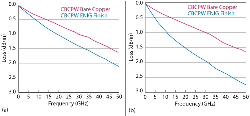
Figure 8 The effect of ENIG on insertion loss of microstrip (a) and GCPW (b) circuits using 8 mil thick RO4003C™ laminate.
References
- John Coonrod, “Comparing Microstrip and CPW Performance,” Microwave Journal, July 2012.
- John Coonrod, “Methods for Characterizing the Dielectric Constant of Microwave PCB Laminates,” Microwave Journal, May 2011.
- Allen F. Horn, III (Rogers Corp.), John Reynolds (Rogers Corp.) and James C Rautio (Sonnet Software), “Conductor Profile Effects on the Propagation Constant of Microstrip Transmission Lines,” IEEE Transactions on Microwave Theory and Techniques Symposium, June 2010.