

Electromagnetic interference (EMI) can plague even the best RF/microwave designs and requires careful planning to control. Designers working with electromagnetic (EM) fields are constantly faced with the threat of stray EM energy leaking into other parts of a circuit or system. EMI can disrupt the performance of the circuit where it originates as well as nearby circuits and systems. Two approaches can reduce or shield EM emissions from a device or system and improve its immunity. The first is shielding the printed circuit board (PCB) through proper design techniques. The second is placing the device or system in a shielded enclosure.
Orbel Corp. produces shielding products for both the printed circuit board (i.e., board-level shielding) and system (i.e., gasketing). Device manufacturers rely on shielding suppliers like Orbel for the technical capabilities and knowledge needed to suppress EMI, since shielding remains challenging.
Board-Level Shielding
A board-level shield can be viewed as a five-sided can. Available in unlimited sizes, shapes and heights, board-level shielding (BLS) is placed around the component or circuit on the printed circuit board that needs to be shielded. The shield restricts to acceptable levels the electromagnetic energy propagating between the source and a receptor. BLS can be manufactured in one-piece, two-piece, multi-cavity and custom configurations. When designing and manufacturing BLS, consider the following to achieve the most effectiveness:
Near field effects: When the shield is in the near field of the source, shielding performance will be affected by the frequency, field configuration, position of the source and distributed inductances and capacitances. The coupling of the source to the shield, the effect of mutual coupling between elements, shield termination and grounding technique all need to be taken into account.
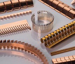
Figure 1 BeCu gaskets from Orbel provide high EMI shielding effectiveness and are available in a variety of finishes.
Layout and hole considerations: The effectiveness of BLS is highly dependent on the proper design of the printed circuit board mounting area. Normally, the sixth side of this “can” will be a ground plane on the board. The number and spacing of traces, vias and holes running from the shielded area to other board components will determine the effectiveness of BLS.
Resonances: Another issue with higher frequencies is the resonance effect, meaning coupling as a consequence of the self-resonance of various structures. For example, the first-order mode of a 2 × ½ - inch enclosure is about 12 GHz. Even weak coupling at these high frequencies can induce strong oscillations that couple to other points in the enclosure.
Thermal management: As devices become faster, they generate more heat. Hence, thermal management is also a design factor. Thermal management can be achieved through the use of thermal pads and heat sinks. Companies like Orbel can assist with design options.
Gasketing
Gasketing maintains shielding effectiveness through proper seam treatment. In general, seams account for most of the leakage in an enclosure design. The shielding effectiveness of a seam depends on materials, contact pressure and surface area. Gaskets maintain conductive contact across mating surfaces. A solution to radiated problems is to make all seams of adjoining metal pieces continuous. If there is no continuity between metal pieces, a radiating aperture for RF is created. This is where gasketing can be used. Chosen based on specific shielding effectiveness requirements, application atmosphere and spatial specifications, both beryllium copper (BeCu) gaskets and metalized fabric gaskets can be used to ensure maximum EMI compliance.

Figure 2 Metalized fabric gaskets are manufactured with a polyurethane foam core and nickel-plated copper-conductive fabric.
Beryllium copper gaskets: BeCu gaskets (see Figure 1) offer the highest level of attenuation over the widest frequency range and are useable in both compression and shear applications. Solid fingers have greater cross-sectional area, hence higher conductivity. The finger shape has the characteristics of an interconnecting ground plane with a large contact area; therefore, the inductance will be low. The slots between the fingers can create potential problems, depending on the frequency range. At sufficiently high frequencies, these slots begin to permit RF energy transmission through the bounded slot configuration.
Metalized fabric gaskets: These gaskets are made of conductive fabric material over foam (see Figure 2). Conductivity can be very low and hence offer very high attenuation, the amount determined by the level and matrix of the conductive particles and the compression force. Gaskets come in various styles and shapes (e.g., rectangular, square, D, bell, knife) that allow compression ranges down to low values.
Since 1961, Orbel’s custom design and manufacturing process has enabled unique engineered solutions for a variety of applications and industries. From conception through delivery, Orbel offers today’s most effective EMI/RFI shielding, photo-etched precision metal parts, precision metal stampings and electroplated metal foils. Areas of specialization include RF/microwave, aerospace, telecommunications, electronics, medical, automotive and manufacturing.
Orbel Corp.
Easton, Pa.
www.Orbel.com