
AlGaN/GaN high electron mobility transistors (HEMT) are designed and fabricated based on 0.15 µm gate-lengthtechnology. All source electrodes of multi-finger devices are connected to the through-hole ground instead of using air bridges. Device RF measurements show that they can operate at millimeter wave frequencies. Parasitic and intrinsic parameters of the small signal equivalent circuit model are extracted at reverse cut-off and operating bias state. The revised Angelov expressions are adopted to describe nonlinear characteristics, and the large-signal model is constructed using the symbolically defined device (SDD) method. Using these devices, a two-stage, four-channel monolithic microwave integrated circuit (MMIC) power amplifier is realized with 36 dBm output power, 9 dB power gain and 10 percent power-added efficiency (PAE) at 34 GHz.
The AlGaN/GaN HEMT is well suited for use in high frequency power amplifiers due to its high two dimensional electron gas (2DEG) concentration, high mobility and high saturation drift velocity. It can also withstand high operational supply voltages and temperatures.
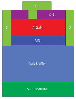
Figure 1 Single-finger AlGaN/GaN HEMT cross section.
Because high imaging resolution and system miniaturization are achievable at millimeter wave frequencies, power amplifier research and design using millimeter wave GaN HEMTs and MMICs has attracted a great deal of international interest.1 Its potential, however, is difficult to realize since GaN technology is complex and immature in the millimeter wave region. Breakdown voltage, output power and power-added efficiency (PAE) are greatly reduced as device physical dimensions become smaller.
This article describes a set of processes for the fabrication of AlGaN/GaN HEMTs and the establishment of equivalent circuit models for a millimeter wave power amplifier. We first design the multi-finger 0.15 µm gate-length GaN HEMTs with an improved source-ground structure and evaluate their frequency characteristics for the millimeter wave application. We then complete parameter extraction of the small-signal equivalent circuit model and construct the large-signal model. Finally, we design, fabricate and measure a two-stage four-channel MMIC power amplifier.
Device Design and Fabrication
A cross-sectional view of a single-finger AlGaN/GaN HEMT structure is shown in Figure 1. The HEMT is grown on a SiC substrate using metal organic chemical vapor deposition (MOCVD). The GaN buffer layer provides lattice matching with the substrate and exhibits high resistance characteristics. The AlGaN barrier layer is unintentionally doped. The 1 nm thick AlN layer is inserted between the barrier layer and buffer layer to increase the 2DEG in the channel. The SiN passivation layer is added to restrain surface defects in the barrier layer.
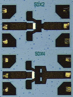
Figure 2 Photograph of two and four finger GaN HEMTs.
The T-gate composed of a Ni/Au alloy is defined using electron-beam lithography. The gate length is 0.15 µm and the gate-cap length is 0.5 µm. The gate-drain cap is longer than the gate- source cap in order to decrease the electric field in the barrier layer and channel. A Ti/Al/Ni/Au alloy is evaporated to form source and drain electrodes through rapid thermal annealing. The ohmic contact resistance is 0.3 ohm-mm. The source-drain distance is optimized to be 3.5 µm.2 Through-hole ground technology is used with all the source electrodes connected to the holes. This new structure solves the source ground problems of multi-finger HEMTs that employ air bridges, reducing source parasitic inductances. Photographs of two finger and four finger devices with 50 µm single-finger gate-widths are shown in Figure 2.
S-parameters of the two HEMTs are measured from 0.1 to 50 GHz at Vgs = -2.5 V and Vds = 20 V respectively. Assuming input and output matching, maximum available gain (MAG) is calculated using the S-parameters and is shown in Figure 3. It is apparent that there is little difference between the two finger and four finger devices, indicating that the multi-finger HEMT does not increase source inductance. The MAG of the two finger HEMT can reach 9.6 dB at 30 GHz while that of the four finger HEMT can reach 10.2 dB. This rise may be due to paralleling of the parasitic resistances.
Equivalent Circuit Model
To design an amplifier, the device equivalent circuit model must be derived. This requires de-embedding of coplanar waveguide (CPW) test pads and lead wires. The thru-reflect-line (TRL) method is used, employing the three calibration structures shown in Figure 4.3 The S-parameters of the core device are determined after de-embedding.
The small-signal equivalent circuit model is shown in Figure 5. Lg, Ld and Ls are parasitic lead inductances of the GaN HEMTs. Rg, Rd and Rs are parasitic resistances. Cgs, Cgd, Cds, Ri, Rds, Gm and t are intrinsic parameters which are related to the gate and drain voltages. All of these parameters can be determined for different bias voltages. The reverse cut-off method is used to extract the parasitic inductances and resistances. Parasitic parameters are ignored when the frequency is lower than 5 GHz at Vgs = -6 V and Vds = 0 V. Under this condition only Cgs, Cgd and Cds exist in the intrinsic region and they are easily obtained. Then the frequency is increased to 50 GHz to obtain the parasitic inductances and resistances. The intrinsic parameters are determined at Vgs = -2.5 V and Vds = 20 V based on Y-parameters, after removing all the parasitic parameters.
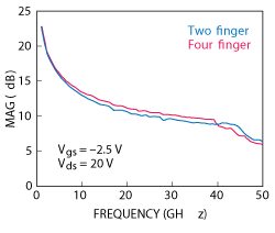
Figure 3 Small-signal gains at Vgs = –2.5 V and Vds = 20 V.
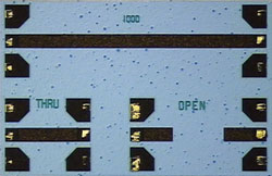
Figure 4 TRL calibration structures.
Nonlinear characteristics are determined by fitting nonlinear expressions at different gate and drain voltages. The Angelov empirical formulas can be used to describe the I-V and C-V large signal property of GaN HEMTs:4

Figure 5 Small-signal equivalent circuit model.


Figure 6 SDD large-signal equivalent circuit model.
Imax and Vmax are the source-drain current and gate voltage when the transconductance reaches the maximum. Cgs0 and Cgd0 are the gate-source and gate-drain capacitances at zero bias. The other parameters in the formulas are fitting coefficients. For the high order polynomials, the needed precision can be satisfied by evaluating them to the third order. The I-V formula should be modified, however, to reflect self-heating under diverse gate voltages. It is revised as follows:

Here, it is mainly considered that the gate voltage should be added to the section that describes saturation characteristics for this change. Other intrinsic parameters have little impact at different gate voltages, so average values may be used.
The large-signal equivalent circuit model with nonlinear fitting expressions can be implemented by using the SDD form during the circuit design process (see Figure 6). Based on the port voltages and currents, this method can reflect large signal characteristics as the intrinsic parameters change along with the bias voltages. The model parameters of multi-finger and different gate-width GaN HEMTs can be obtained through parallel and linear relationships.5
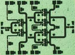
Figure 7 MMIC power amplifier.
Power Amplifier MMIC Realization and Measurement
The MMIC power amplifier is designed and fabricated using the multi-finger GaN HEMT equivalent circuit models. In addition to the active devices, some passive components such as microstrip lines, capacitances, resistances and through-holes are needed. The equivalent circuit models of these passive devices are obtained through 3-D electromagnetic simulation.
The MMIC is designed with a two-stage, four-channel topology.6 The front end combines two 8 × 60 µm GaN HEMTs. The output stage consists of four 8 × 75 µm GaN HEMTs. The matching circuits of each stage are optimized based on the source and load-pull method. The input and output ports are CPW, and the port impedances are matched to 50 ohms. Stability measures are incorporated to prevent self-oscillation. The fabricated circuit is shown in Figure 7. Its total area is 3.3 × 2.5 mm.
The MMIC is measured on wafer. The 24 V drain bias supply is pulsed with a 10 µs pulse width and 10 percent duty cycle, and the gate bias is set to -2.5 V for both stages. With an input power of 27 dBm under CW operating conditions, the measured performance is shown in Figure 8. The output power is higher than 33 dBm over the entire 33 to 35 GHz band, and the maximum output power is 36 dBm at 34 GHz with 9 dB gain and 10 percent PAE.
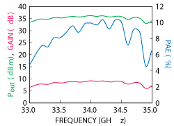
Figure 8 MMIC power amplifier measured performance.
Conclusion
Multi-finger 0.15 µm gate-length AlGaN/GaN HEMTs designed with improved source electrode structures effectively solve the grounding problems of multi-finger HEMTs employing air bridges. A GaN MMIC power amplifier designed using these devices yields 36 dBm output power, 9 dB power gain and 10 percent PAE at 34 GHz.
Acknowledgment
This work is supported by the Beijing Higher Education Young Elite Teacher Project.
References
- R.S. Pengelly, S.M. Wood, J.W. Milligan, S.T. Sheppard and W.L. Pribble, “A Review of GaN on SiC High Electron-Mobility Power Transistors and MMICs,” IEEE Transactions on Microwave Theory and Techniques, Vol. 60, No. 6, June 2012, pp. 1764–1783.
- S. Russo and A. Carlo, “Influence of the Source–Gate Distance on the AlGaN/GaN HEMT Performance,” IEEE Transactions on Electron Devices, Vol. 54, No. 5, May 2007, pp. 1071–1075.
- G.F. Engen and C.A. Hoer, “Thru-Reflect-Line: An Improved Technique for Calibrating the Dual Six-Port Automatic Network Analyzer,” IEEE Transactions on Microwave Theory and Techniques, Vol. 27, No. 12, December 1979, pp. 987–993.
- I. Angelov, H. Zirath and N. Rorsman, “A New Empirical Nonlinear Model for HEMT and MESFET Devices,” IEEE Transactions on Microwave Theory and Techniques, Vol. 40, No. 12, December 1992, pp. 2258–2266.
- Z. Valiallah, P. Yi, U.K. Mishra and R.A. York, “A Scalable EE-HEMT Based Large Signal Model for Multi-Finger AlGaN/GaN HEMTs for Linear and Non-Linear Circuit Design,” Physica Status Solidi C: Current Topics in Solid State Physics, Vol. 7, No. 10, July 2010, pp. 2450–2454.
- C.F. Campbell, M.Y. Kao and S. Nayak, “High Efficiency Ka-Band Power Amplifier MMICs Fabricated With a 0.15 µm GaN on SiC HEMT Process,” 2012 IEEE MTT-S International Microwave Symposium Digest, June 2012, pp. 1–3.