
S-parameters and the network analyzer transformed how RF and microwave engineers share information, enabling them to accurately describe the electrical properties of complicated networks with a simple “black box.” This allowed component suppliers and modeling teams to provide comprehensive design information: passive element data (inductors, vias and IC packages) for MMIC/MIC designers and radio blocks (amplifiers, attenuators, filters and couplers) for system integrators. The ability to share device characteristics and protect design IP accelerated the evolution of wireless products and the growth of the supply chain. Today’s technology trends and market opportunities require even greater levels of component integration, which call for smaller, lighter, less expensive and wider bandwidth products. These products cannot be represented accurately nor efficiently designed using black boxes that fail to capture their electrical interactions with the surroundings.
To simulate the real world performance of highly integrated devices, designers must account for the electromagnetic (EM) coupling and parasitic behavior resulting from their close proximity to other structures. While high frequency and high speed designers have addressed this with EM simulation, the equivalent of an IP protected, “electromagnetic aware” black box has not existed. In addition, developing tomorrow’s wireless electronics requires that multi-disciplinary engineering teams share and incorporate physics-based models in larger complex systems, using a collaborative workflow to meet the electrical, thermal and mechanical requirements. To address all these needs, ANSYS is introducing version 16.0 with the new ANSYS Electronics Desktop featuring ANSYS HFSS and the industry’s first 3D EM component library (shown in Figure 1).

Figure 1 The ANSYS Electronics Desktop unifies HFSS, Q3D Extractor, HFSS 3D layout, PlanarEM, Circuit and System analysis into a single, unified environment that allows drag-and-drop dynamic links between electromagnetic and circuit simulation.
The pending pervasive connectivity of electronic devices (known as the Internet of Things or IoT), compounded by physical design challenges such as through-silicon via (TSV) stacked die and complex multi-chip and multi-package integration (known as more-than-Moore), impose a higher standard for hardware and software reliability.
ANSYS 16.0 answers this challenge with a new platform of integrated solver technologies and automation. ANSYS 16.0 meets the increasing demands for electronic reliability and performance, both throughout the design process and across a diverse electronics supply chain.
Electronics Desktop
The new ANSYS Electronics Desktop in version 16.0 is a single environment with a highly integrated interface that provides a streamlined workflow between ANSYS EM field solvers, circuit/system simulators, ECAD links, and EMI/EMC compliance reporting. The integration aids physics-based, first-pass design success. This new platform delivers a single desktop for HFSS, HFSS 3D Layout, HFSS-IE (integral equation solver), Q3D Extractor (quasi-static), Planar EM, Circuit and System simulations. Users can insert HF/SI analysis into coexisting projects with drag-and-drop dynamic links between the EM and circuit simulations. This yields simple problem set-up and reliable performance.
Today’s designs are often developed hierarchically from legacy and new building blocks. ANSYS 16.0 introduces the ability to create 3D EM components and integrate them into larger assemblies and systems. These include multi-pin connectors, phased arrays and highly-integrated chip-package-board systems. This capability is especially useful for sharing detailed device models within an organization and between supplier and system integrators. Simulation-ready 3D components can be created and stored in library files, then easily added to larger system designs without needing to apply excitations, boundary conditions and material properties. This leverages the existing information to save engineers valuable set-up time and ensure accurate data entry. All the internal details are incorporated in the original design of the 3D components.
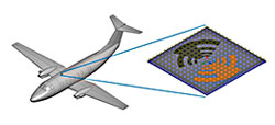
Figure 2 A three-layer satellite antenna modeled as a 3D component in ANSYS HFSS. Given the vastly different scales, the antenna is independently meshed from the aircraft platform to efficiently study antenna placement.
With the wireless industry developing products for the IoT, 5G and commercialized UAVs, there is growing demand for simulation tools that design and integrate devices, antennas, filters and connectors into complex structures such as airframes, appliances, biomedical implants and industrial equipment. ANSYS 16.0 and the new HFSS 3D EM component library target these emerging applications with advanced EM solver technologies and parametric optimization. This enables wireless devices and systems to be simulated from the actual assembly of components and systems. By providing full 3D accuracy to assemblies of varying scale, this latest release accelerates placement studies, ensures robust design to manufacturing variances and supports collaboration through component sharing.
3D Component Libraries
The efficient use of the 3D component libraries requires information sharing beyond just geometries. The mesh assembly allows antennas and other parts of the design to be modified without re-meshing the entire structure, which speeds design studies and optimization. For example, IoT designs include antennas placed on equipment, the human body, buildings, base stations and other structures. UAVs have multiple antennas on complex airframes made of composite materials. The 3D component libraries help system integrators solve such complex antenna location problems. Figure 2 shows an example of a thin three-layer antenna, which includes frequency selective surfaces, that can be meshed independently, then placed on the aircraft for efficient placement trade-offs.
The 3D component library models allow encryption to protect collaboration throughout the design chain –
potentially an industry changing paradigm. Component modeling with encryption allows users to password protect their component design so that it can be securely shared. Designers can capture the EM interaction between components, which is more accurate than cascading S-parameters and not accounting for the EM interaction. This capability allows specialized designs of antennas and components such as high speed connectors to be used by designers with less experience in RF design.
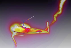
Figure 3 New capabilities in the HFSS Transient solver make it easy to simulate time domain scenarios, such as ESD and lightning strikes on aircraft.
Additional HFSS Solver Enhancements
ANSYS 16.0 includes several notable enhancements to its HFSS best-in-class EM solver technology. The HFSS Transient option has been upgraded with a new implicit finite element time domain (FETD) technique for simulating time domain scenarios. FETD is especially powerful for electrically small problems, such as lightning strikes on aircraft (as shown in Figure 3), electrostatic discharge (ESD) and time domain reflectometry. The implicit solver provides unconditionally stable time marching, with the time step not limited to the smallest geometric detail. Addressing the challenge of simulating an antenna mounted on a much larger and complex structure, the HFSS-IE solver now includes a powerful multilevel fast multipole method (MLFMM) solver. MLFMM is fast and efficiently uses memory when analyzing problems with extreme electrical dimensions, i.e., more than one hundred wavelengths.
ANSYS 16.0 enhances EM and multiphysics solvers through a new, fully integrated Electronics Desktop with encrypted 3D component libraries. Using these improved tools, RF/microwave designers will be successful addressing the next level of wireless product complexity and system integration.
ANSYS Inc.
www.ansys.com