
Chip-size Package Technology for Semiconductors
Chip-scale packaging (CSP) of IC devices is rapidly gaining acceptance worldwide because of intrinsic size advantages, the promise of highly favorable cost/performance trade-offs and reliance on existing materials and assembly infrastructures. The compliant, flex-circuit-based package is increasingly being viewed as the CSP method of choice. Flex-circuit-based, chip-size packages that are not significantly larger than the chip outline itself are available, enabling dense packaging of components and short interconnection distances, resulting in lower inductance and reduced parasitics. Ball-grid array (BGA) CSPs are compatible with most surface-mount assembly operations and have the testability of a traditionally packaged die.1 These package design attributes make the flex-based CSP an attractive die packaging solution for high frequency applications as well as high speed digital devices. Activities are also underway to utilize the chip-size BGA package to interconnect semiconductors at the wafer level where the totally integrated IC can be fabricated and tested in its final configuration while still on the wafer. This article reviews a novel chip-size BGA package construction, process flow and reliability data. Results of simulations and measurements of high frequency signal characteristics on the package and through the interconnects are discussed, along with potential applications for CSPs in the wireless industry.
David Light, Anthony Faraci and Joe Fjelstad
Tessera
San Jose, CA
Flip-chip assembly (FCA) technology has long been perceived as the ultimate solution for interconnecting die. Board space is minimized, electrical and thermal performance is enhanced and die packaging costs are avoided. In reality, the assembly infrastructure for flip-chip use in the merchant market is in the very early stages of development. Additionally, the availability and cost of known good die, FCA reliability issues and difficulties associated with testing bare die and reworking encapsulated flip-chip die are significant issues inhibiting the widespread implementation of flip-chip modules (and multichip modules (MCM)). Consideration of replacing or supplementing the existing SMT infrastructure with an FCA and bare die test infrastructure represents an enormous capital investment and forces an assessment of alternative interconnect solutions compatible with existing assembly tooling.
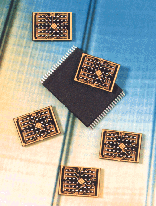 CSPs are the same size (or nearly so) as the die itself. Their performance is superior to high pin count plastic alternatives such as quad flat packs due to reduced lead inductance, simultaneous switching noise, cross talk and address-access time. In fact, CSP performance approaches that of bare die and enables the use of lower voltages and higher speeds.1 The CSPs’ small footprint alone, as shown in Figure 1 , is an overriding benefit for space-sensitive applications such as Personal Computer Memory Card International Association (PCMCIA) cards, smart cards, camcorders, mobile telephones, portable Global Positioning System (GPS) receivers, pagers, personal digital assistants (PDA) and laptop computers.
Cost remains a critical parameter for almost all applications. The cost metric typically used today is pennies per lead. However, to effectively assess the relative costs of the competing interconnect technologies of flip-chip, CSP, MCM and standard single-chip packages, the value of package footprint area, weight, function, testability, assembly infrastructure and reliability, and the costs of assembly and test processes and materials also must be accounted for. In this context, the pricing of CSPs compares favorably with the alternatives, with the flex-circuit-based packages projecting the lowest costs. Additionally, chip-size packaging enables wafer-level packaging, which is the ultimate efficient, low cost packaging format.
The earliest adoption of CSPs is projected in Japanese-produced, space-sensitive consumer products such as PCMCIA cards, camcorders, mobile telephones, smart cards and PDAs. Follow-on applications are expected to include automotive electronics, portable computers, wireless equipment and appliances. Part of the driving force for CSPs in Japan is the quest for higher memory capacity, which requires lighter packages utilizing less area on the printed circuit substrate, particularly for 64 and 256 MB dynamic random-access memories.2
Package Construction
The construction of a compliant, flex-circuit-based CSP is shown in the cross section in Figure 2 .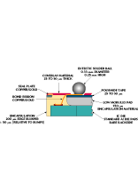 The die is attached adhesively to a flexible, polyimide-based circuit via an elastomeric material. This elastomer serves to decouple the die from the solder balls and printed circuit substrate mechanically, accommodating the coefficient of thermal expansion (CTE) mismatch between silicon and copper/
 FR-4 by yielding elastically. The electrical interconnection between the die and the solder ball on the package is accomplished by bonding plated leads on the flexible circuit to the die pad thermosonically. The package bond lead also has been designed to accommodate relative movement of the package and die, as shown in Figure 3 . It is shaped during bonding into an S with relatively large radii, reducing stress concentration at the heel of the bond where wire bond fatigue failures typically occur.
The bond leads and die edges are fully encapsulated in elastomer following bonding. This construction serves to distribute strain more uniformly along the length of the lead and protects the edges of the die during handling at test and surface-mount assembly of the package to the board. The compliant polymeric elastomer decouples the thermal expansion of the printed wiring board (» 18 ppm/°C) from that of the die (» 3 ppm/°C).
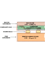
In contrast, FCA requires a void-free, rigid underfill to mitigate stress by creating a bimetal equivalent thatwarps the substrate and/or die during thermal cycling to redistribute stress. Processing challenges to this approach are significant and include the need for a void-free encapsulant with good adhesion to the package and PCB. Die cracking can be induced by the warpage imposed on the die during thermal cycling. Figure 4 shows a schematic comparison of the BGA package and a flip-chip attached die.
Packaging Materials
The base material for the compliant chip-size package is a polyimide-based flexible circuit. For low input/output (I/O) applications such as flash memory, single-metal tape-augmented-bonding (TAB)-type tape is adequate and is available from a number of suppliers worldwide. For higher I/O and higher performance applications, two-metal layer flex materials are necessary to increase wireability or improve impedance control and reduce cross talk. For these high I/O applications, processing technology has been developed to produce high density, high reliability microflex circuits in volume.
Currently, the elastomeric die attach and encapsulant material is silicone based and provides good compliance (low modulus), high temperature capability, low ionics and good moisture resistance. This CSP has demonstrated compatibility with JEDEC level one moisture preconditioning. Additional elastomeric materials are currently in development, including filled silicones, flexible epoxies and fluoropolymer-based materials.
Solder balls for the BGA interconnection from package to circuit board can be standard eutectic solder (0.33 mm in diameter and 0.25 mm high). Because of the compliant interface between the die and package, this CSP also enables the use of copper-core solder balls, which can enhance testability of the package. The solder pads are 0.3 mm and protected by a 0.4 mm diameter solder mask (standard dry film material). Bump pitch ranges from 0.5 to 1 mm. For single-metal flex tape, traces, bumps and bond leads are located on the same side of the polyimide. For two-metal flex materials, the traces are located on the die side of the polyimide, and solder balls and reference planes (or additional traces for escape of high I/O die) are located on the other side of the polyimide. In either case, the backside of the die is exposed for enhanced thermal dissipation.
The Assembly Process
Assembly of the compliant, chip-size BGA package is similar to that for TAB devices. An advantage of this package is that the ribbon leads are supported at both ends up to the moment of bonding. The base for the assembled package, as described previously, is a compliant mounting tape produced as a microflex circuit material on polyimide.
Assembly of the package is performed in standard 35 mm-wide strips; future formats will include 70 mm strips and larger. The equipment is typical of that found on most plastic IC assembly lines. Die attach, lead bonding, encapsulation, solder ball and test units are off the shelf from multiple suppliers, requiring only unique motion-control software and parts fixturing.
Assembly begins with die attach using the elastomeric die attach and stand-off materials described previously. Following die attach, lead bonding is performed using standard wire bonders, the only difference being specific software for head motion and the bonder capillary for the CSP. Thermosonic bonding parameters are die pad/lead configuration and metallurgy specific, and are optimized through design of experiments (DOE). Following lead bonding, solder mask is applied using vacuum lamination, exposed and, after encapsulation, developed to expose the pads for solder ball attachment. Encapsulation is performed by robotic dispensing equipment. A new vacuum encapsulation technology and supporting equipment accelerate the encapsulation process and eliminate voids under the die. Solder balls are placed on the entire strip through a stencil after flux screening and then passed through a standard reflow oven. This process is followed by flux cleaning, testing for opens and shorts, marking on the exposed backside of the die and singulation of the packaged die into individual CSPs.3
Reliability
Typical reliability requirements for semiconductor packaging have been dictated by MIL-STD 883. The tests prescribed by this standard are demanding, but passing this standard assures the end user of the package a high degree of reliability. General qualification test conditions for electronic packaging are listed in Table 1 . These tests include evaluation of the free-standing package as well as testing of the package surface mounted to an FR-4 circuit board.
|
Table I | ||
|
Test Required |
Conditions |
Duration |
|
High Temperature Storage |
150° C |
1000 hours |
|
Thermal Cycling on FR4- condition B° |
-55° C to 125° C |
1000 cycles |
|
Thermal Shock - condition C° |
-65° to 150° C |
500 cycles |
|
Steam Pressure Test |
121° C at 2 atm |
168 hours |
|
Temperature and Humidity under bias |
85° C/85% RH |
1000 hours |
|
° Parts are preconditioned at JEDEC level 1 | ||
Memory die interconnected using this package construction with gold bonding leads have achieved the listed reliability requirement in testing performed by the supplier and various end users.4 Packages with copper bonding leads have achieved 500 cycles of Condition B thermal cycling on FR-4. This package’s JEDEC level one preconditioning results are a significant improvement over all existing organic surface-mount packages available in the industry. The package design intrinsically decouples the die from the printed wiring board mechanically, reducing stress on the solder joints dramatically. In addition, the compliant S-shaped bonding leads accommodate the differential movement of the package components during thermal cycling. The moisture resistance can be attributed to the low moisture absorption of the silicone encapsulant and die attach material.
Modeling performed previously predicted approximately a 60 percent-longer field life for this package attached to an FR-4 circuit board without underfill vs. a flip-chip attached die with underfill.3 These models were verified with numerous reliability studies.
Electrical Performance
The electrical performance of this chip-scale BGA package benefits by its small outline and thin profile. Signal path length is decreased, reducing parasitics including mutual inductance and capacitance while minimizing simultaneous switching noise and address-access time. While these attributes have played a key role in the choice of this package for memory die and future processor interconnects, they also indicate a probable advantage for interconnect of high frequency die for many wireless applications. To better understand the applicability of this CSP to high frequency die interconnects, a case study simulation was performed on single-metal and two-metal (with ground plane) packages. In addition, sample single-metal packages were fabricated and assembled. Measurements were performed to extract the electrical parasitics from a typical 48 I/O chip-scale BGA package.
Simulation Case Study
A case study was analyzed using a three-dimensional (3-D)/two-dimensional (2-D) modeler. Electrical attributes of single- and double-metal CSP BGA packages were characterized. In the two-metal case, the second metal is used as a ground plane. For both package types, the 3-D simulator was used only on the bond ribbon; the remainder of the package was modeled in 2-D.
|
Table II | |||||
|
Physical Dimensions |
Lead Length 350 m m |
Bond Area |
Lead Height |
Lead Pitch |
TV-46 Tapered Lead Style |
|
Lself (nH) |
Lm+1 (nH) |
Lm+2 (nH) |
Lm+3 (nH) |
Lm+4 (nH) |
RB1 (W ) |
|
0.22 |
0.091 |
0.056 |
0.040 |
0.031 |
0.008 |
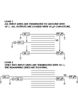
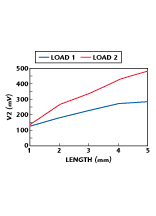
For this model, the package is simulated as attached to an FR-4 board (0.031 mil, 0.8 mm). The 3-D modeler extracted the inductance and resistance of a gold-coated copper bond ribbon. The results are listed in Table 2 . The extracted bond ribbon data were used in all of the remaining circuit simulations. The extraction of the circuit trace parasitic was performed with the 2-D modeler using the single-metal construction shown in Figure 5 , with results listed in Table 3 . Circuit simulations also were performed on a 10-trace circuit with and without capacitive loading and input loading. The circuit configuration is shown in Figure 6 . From this configuration, an upper and lower limit for cross talk can be determined as a function of trace length. A plot of cross talk vs. trace length is shown in Figure 7 using an input source of 0 to 2.5 V with a 200 ps risetime.
_
|
Table III | |
|
Lself (nH) |
0.520 |
|
Lm ± 1 (nH) |
0.258 |
|
Ctotal (fF) |
109 |
|
Cp (fF) |
16 |
|
Cside x 2 (fF) |
88 |
|
(Lself /Ctotal )0.5 ( W ) |
69 |
|
Ctotal = Cp (parallel plate capacitance) Lself = self-inductance of a trace surrounded by four traces per side L m ± 1 = mutual inductance with respect to the center trace (only one coupling pair is shown) | |
In the two-metal package construction, the trace metal is located on the underside of the polyimide flex (between the flex and die). This construction requires vias to connect the traces to the solder pads on the second metal layer. The second metal is also used to form a ground plane above the trace metal. Figure 8 shows the material cross section input to the 2-D modeler and Table 4 lists the results.
|
Table IV | |||||
|
Lself |
Lm ± 1 |
Ctotal |
Co |
Cside x 2 |
(Lself /Ctotal )0.5 |
|
0.315 |
0.088 |
132 |
59 |
72 |
49 |

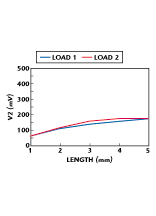
 Cross-talk simulations also were performed as a function of trace length and load for the two-metal layer package shown in Figure 9 . The results are shown in Figure 10 for the same 0 to 2.5 V input. Signal trace propagation also was compared between the one- and two-metal constructions.
In summary, a 20 percent improvement in performance (propagation delay) and a 40 percent reduction in cross talk are realized by inclusion of a second metal layer consisting of a ground plane in the compliant, flex-circuit-based chip-size BGA package.
Measured Electrical Data
The measurement methods employed to extract the electrical parasitic from a 48 I/O single-metal chip-size BGA package are described. The results are summarized and compared to the simulation case for a single-metal package described previously.
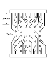 Figure 11 shows a top view of a TV-46 48 I/O daisy-chain test die. Selected traces were chosen for measurement while the remaining unused traces were connected to an internal ground. No floating traces were allowed, thereby
 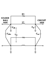 eliminating erroneous resonance. The package dimensions are 7.868 ¥ 5.760 mm; the longest trace is 2.5 mm. Trace width is 0.05 mm and trace space is 0.05 mm for 2.0 mm length, with the remaining route at or greater than 0.075 mm.
A SPICE™-compatible equivalent-circuit model was extracted, as shown in Figure 12 , using the HP MDS where
L1* = self inductance of trace line
Lm * = mutual inductance between adjacent trace lines
Cp * = capacitance of the trace line
Cm * = mutual capacitance between two adjacent trace lines
R1 = shunt resistance of L1 (used to model high frequency loss due to skin effect and dielectric loss)
Csb = capacitance of solder ball land (fixed at 300 mm)
Csbc = capacitance between adjacent solder balls (fixed at 0.75 mm pitch).
(*These parameters scale linearly up to 5 mm trace lines.)
 The approach used defined the die surface as ground.6 In this test package, the compliant chip-size package was bonded to a
  thin-film surrogate ceramic chip. All unused signal traces on the package are bonded to this common ground plane. To reduce resonance further, a fixture was designed to provide an additional ground plane for the test probes. All parasitics introduced by the fixture in this way are nulled.
Selected minimum-, intermediate- and maximum-length signal trace pairs were analyzed. For each trace length pair, three configurations were tested: open-, shorted- and loop-through pairs. The measurements were taken as scattering (S) parameters. All measurements were performed using Picoprobes (designed  to provide a high quality 50 W path for high frequency measurements) along with the model HP8510C network analyzer (frequency domain).
Tables 5 and 6 show the extracted model parameters. Self-inductance and capacitance as a function of trace length are shown in Figures 13 and 14 , respectively. The bandwidth of the package was measured in loop-through configuration on pins E6 to F6. As shown in Figure 15 , the first dip occurs at 5 GHz. The derived SPICE model appears valid from DC to over 4 GHz (AC performance only, no IR drop is modeled). The model-simulated cross talk is within 0.5 dB of actual measurements. A short- and open-circuit measurement for a long trace pair (2.8 mm) was performed. The Smith charts shows good agreement with the model.
|
Table V | ||||
|
Pins |
Csb (pF) |
Cp (pF) |
L1 (nH) |
R1( W ) |
|
Long traces: 2.8 mm, E1, E6 |
0.05 |
0.20 |
1.30 |
2000 |
|
Mid1-length traces: 2.0mm, F1, F2, C1, C6, F5, F6 |
0.05 |
0.12 |
0.93 |
2000 |
|
Mid2-length traces: 1.2mm, B1, B2, G2, B5, B3, G5 |
0.05 |
0.09 |
0.66 |
2000 |
|
Short-length traces: 0.375mm, A2, A5, A3 |
0.05 |
0.04 |
0.34 |
2000 |
|
Table VI | |||
|
Pins |
Csbc (pF) |
Cm (pF) |
Lm (mH) |
|
Long-traces: 2.0mm |
0.01 |
0.040 |
0.12 |
|
Midlength trace pairs :1.2mm |
0.01 |
0.033 |
0.07 |
|
Short-trace pairs: 0.375mm |
0.01 |
0.016 |
0.04 |
Conclusion
Chip-scale and chip-size packages are revolutionizing the way die are packaged. Acceptance of these new technologies is occurring at a remarkable rate as a result of their small form factor, improved electrical performance and competitive costs. The compliant, flex circuit-based CSPs have distinguished themselves from other chip-size packages by providing a robust and reliable package in a true chip-size format. The minimalist format of these packages makes them ideal for size- and weight-constrained applications, including portable wireless communication devices such as mobile telephones, pagers and GPS receivers. Recent simulations and measurements on the compliant CSP indicates performance is good up to 4 GHz on the single-metal packages. Two-metal packages including a reference plane are expected to perform significantly better at high frequency than the single-metal package. Future measurements are planned to assess the double-metal packages.
Acknowledgment
The electrical data measurements and methods were performed by GigaTest Labs, Cupertino, CA. The HP MDS is a product of Hewlett-Packard Co., Santa Rosa, CA. The Picoprobes are manufactured by GGB Industries, Naples, FL.
References
1. Glenda Derman, "Interconnects and Packaging, Part One: Chip-scale Packages," Electronic Engineering Times, Monday, February 26, 1996.
2. Glenda Derman, "Chip-size Packages Proliferate," Electronic Engineering Times, December 15, 1996.
3. Tom DiStefano and Edwin Heacox, "Designing a Modular Chip-scale Package Assembly Line," Circuits Assembly, March 1997.
4. Tom DiStefano, "Design, Material, Process, Reliability and Manufacturing Transfer of BGA," NEPCON West, February 24, 1997.
5. J. Fjelstad and J.P. Clech, "Reliability Prediction Modeling of Area Array CSPs," Electronic Packaging and Production, June 1997.
6. A.D. Fraser, O.C. Bell and C.T. Strouth, "Electrical Characterization of Ball Grid Array (BGA) Packages," 1996 High Performance System Design Conference.